Flexible PCB Design Guide: How to Avoid Circuit Breaks at Bends
In our flexible circuit projects spanning medical devices to aerospace applications, bend failures account for roughly 40% of field returns during the first year. Most engineers understand the basics—keep bend radius above 10× thickness—but that rule alone won’t prevent cracks in dynamic flex applications cycling 100,000+ times. This guide distills lessons from designs that survived harsh environments versus those that failed within months.
Understanding Flex Circuit Bend Mechanics
When a flexible PCB bends, the copper traces on the outer radius experience tensile stress while inner radius traces face compression. The neutral axis—where stress theoretically zeroes out—sits near the middle of the substrate. However, in multilayer constructions with asymmetric copper distribution, this neutral axis shifts, creating uneven stress patterns that accelerate copper fatigue.
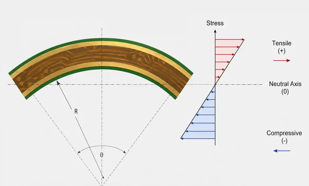
In our automotive sensor flex designs, we’ve measured stress concentrations 3-4× higher at trace corners within bend zones compared to straight sections. This explains why seemingly adequate bend radius specifications still produce failures. The copper’s grain structure also matters—rolled annealed copper elongates 20-30% before fracture, while electrodeposited copper fails at 8-12% elongation.
Key Stress Factors in Bend Zones:
| Stress Factor | Impact on Failure Risk | Mitigation Strategy |
|---|---|---|
| Bend radius reduction | Exponential increase below 6× thickness | Increase radius or reduce stack thickness |
| Copper thickness | Higher stress concentration with thicker copper | Use ½ oz copper in bend areas |
| Trace width variation | Stress risers at width transitions | Gradual taper over 5-10mm |
| Adhesive type | Rigid adhesives crack first | Use flexible adhesive systems |
| Layer count | Each layer adds stiffness | Minimize layers in bend region |
Critical Design Parameters for Bend Regions
The traditional 10× bend radius guideline assumes static bending with 1 oz copper. For dynamic applications—think laptop hinges cycling 50,000 times—we specify 20× minimum radius with ½ oz rolled-annealed copper. This isn’t theoretical conservatism; it’s based on accelerated life testing showing exponential failure rate increases below these thresholds.
Temperature compounds the problem. A flex circuit bending at -40°C experiences 40% higher stress than the same bend at room temperature because polyimide stiffens significantly. Our aerospace designs account for this with oversized bend radii in cold-environment installations, often reaching 25-30× thickness ratios.
Recommended Bend Radius Specifications:
| Application Type | Minimum Bend Radius | Copper Weight | Expected Cycles |
|---|---|---|---|
| Static flex (install once) | 6× total thickness | 1 oz acceptable | < 100 |
| Occasional flex (monthly) | 10× total thickness | ½ oz preferred | 100-1,000 |
| Dynamic flex (daily) | 20× total thickness | ½ oz rolled-annealed | 1,000-50,000 |
| Continuous flex (constant motion) | 25× total thickness | ¼ oz rolled-annealed | > 100,000 |
Copper Selection and Treatment Methods
Rolled-annealed (RA) copper versus electrodeposited (ED) copper isn’t just a cost consideration—it’s a reliability decision. In bend testing at our facility, RA copper lasted 3× longer in dynamic flex applications. The rolling process aligns copper grains parallel to the rolling direction, creating preferential flexibility along that axis.
For designs requiring over 10,000 flex cycles, we exclusively specify RA copper oriented with the grain direction parallel to the bend axis. This requires coordination with your fabricator during panelization. ED copper costs 30-40% less but works acceptably only for static or occasional flex applications below 1,000 cycles.
Copper thickness directly governs flexibility. Each step down in copper weight—from 1 oz to ½ oz to ¼ oz—reduces bending stress by approximately 35-40%. However, thinner copper increases resistance, requiring wider traces to maintain current capacity. This trade-off becomes critical in high-current power delivery applications where you can’t simply reduce copper weight.
Trace Routing Strategies in Flex Zones
The cardinal rule: traces must run perpendicular to the bend axis. Parallel traces experience maximum stress and fail quickly. In practice, achieving perfect perpendicular routing proves impossible when transitioning from one rigid section to another at different orientations. The solution involves creating a transition zone where traces gradually rotate 15-30° before entering the bend region.
Trace width consistency matters more in flex zones than rigid sections. Every width change creates a stress riser where cracks initiate. When you must change width—say, transitioning from a fine-pitch component to a wider power trace—taper the transition over at least 5mm length. Abrupt width changes should never occur within 10mm of a bend zone.
We’ve had success using hatched ground planes rather than solid copper fills in bend areas. A crosshatch pattern with 0.5mm spacing and 0.15mm trace width provides adequate shielding while maintaining flexibility. Solid copper planes create stiff boards that crack at the plane edges during bending.
Dynamic vs Static Flex Design Differences
Static flex circuits—bent once during installation and never moved again—tolerate design compromises that would devastate dynamic applications. You can use tighter bend radii, thicker copper, and even include small rigid sections near bends. Dynamic flex demands stricter discipline across every parameter.
Design Comparison: Static vs Dynamic Flex:
| Design Aspect | Static Flex | Dynamic Flex |
|---|---|---|
| Minimum bend radius | 6-10× thickness | 20-25× thickness |
| Copper type | ED copper acceptable | RA copper required |
| Copper weight | Up to 1 oz | ½ oz or ¼ oz maximum |
| Coverlay in bend | Standard 1 mil | Thin 0.5 mil or none |
| Stiffener proximity | Can be 2mm from bend | Must be 10mm+ from bend |
| Trace orientation | 80-90° to bend | 90° strict perpendicular |
| Ground planes | Hatched or solid | Hatched only, reduced coverage |
| Layer count in bend | Up to 4 layers | 1-2 layers maximum |
The coverlay choice significantly impacts dynamic flex life. Standard 1 mil polyimide coverlay with acrylic adhesive adds stiffness that accelerates copper fatigue. For applications exceeding 10,000 cycles, we specify 0.5 mil coverlay with flexible adhesive, or use inkjet-printed solder mask that adds minimal thickness.
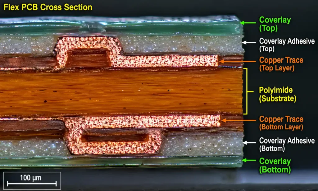
Material Stack-up Considerations
Polyimide substrate thickness drives overall flexibility. Standard 1 mil (25μm) polyimide with ½ oz copper and coverlay yields approximately 0.004″ total thickness. This works well for occasional flex applications. Dynamic flex requiring tight bend radii benefits from thinner 0.5 mil polyimide, though it costs 50-70% more and limits current-carrying capacity.
Adhesive selection often gets overlooked but critically affects reliability. Acrylic adhesives—the industry standard—become brittle below 0°C and soften above 105°C. For extended temperature applications, we specify polyimide-based adhesive systems or adhesiveless constructions where copper is directly deposited onto the substrate.
Multi-layer flex constructions should minimize layers in the actual bend zone. This typically means using rigid-flex designs where the bend region contains only 1-2 flex layers, while rigid sections on either end accommodate additional signal and power layers. Attempting to bend a 6-layer flex stack rarely succeeds in dynamic applications regardless of bend radius.
Testing and Validation Approaches
Accelerated life testing remains the only reliable predictor of field performance. We conduct dynamic bend tests using automated fixtures cycling flex samples through their specified bend radius at 60 cycles per minute while monitoring electrical continuity. A design intended for 10,000 cycles must survive 30,000+ test cycles to account for manufacturing variability and use case uncertainty.
Environmental testing adds another validation layer. Temperature cycling from -40°C to +85°C while flexing reveals adhesive failures and copper embrittlement that room-temperature testing misses. These combined stress tests frequently expose design weaknesses that single-variable testing overlooks.
Recommended Test Protocol for Dynamic Flex:
| Test Type | Test Conditions | Pass Criteria |
|---|---|---|
| Static bend | Minimum specified radius for 1 hour | Zero resistance change (< 1Ω increase) |
| Dynamic flex room temp | 3× target cycles at 60 CPM | < 10% resistance increase, no open circuits |
| Dynamic flex cold | 1× target cycles at -40°C, 30 CPM | < 20% resistance increase, no open circuits |
| Temperature shock | 100 cycles -40°C to +85°C, 15 min dwells | No delamination, < 15% resistance change |
| Combined stress | Flex while temperature cycling | Most severe test, < 30% resistance increase |
Common Failure Modes and Prevention
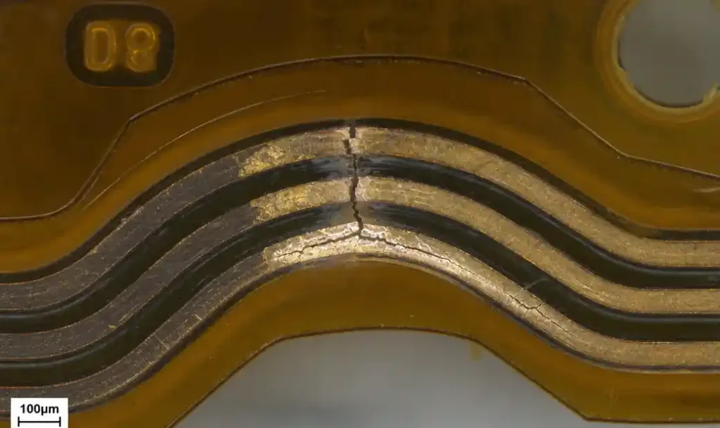
Copper cracking at bend apexes accounts for 60-70% of flex circuit failures we analyze. This typically manifests as intermittent opens during flexing that become permanent after thousands of cycles. Prevention requires adequate bend radius, proper copper selection, and trace routing perpendicular to the bend axis. There’s no single fix—all three must be correct.
Delamination between copper and substrate occurs when adhesive fails under repeated stress. This presents as bubbling or wrinkles in the bend area, often accompanied by discoloration. Switching to high-temperature adhesive systems or adhesiveless constructions solves most delamination issues, though at higher material cost.
Coverlay cracking creates a different failure mode where the protective coverlay splits but copper remains intact initially. However, the exposed copper then oxidizes and eventually cracks. This failure mode is particularly insidious because early-stage cracks in coverlay appear cosmetic but predict imminent electrical failure.
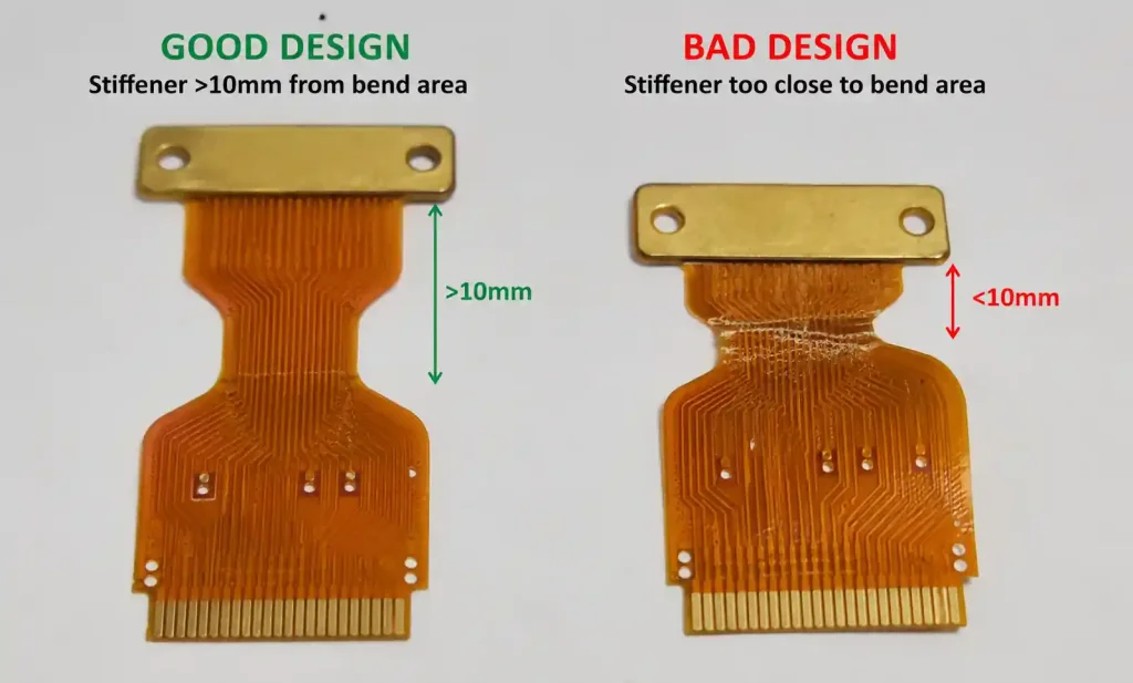
Stiffener encroachment—placing stiffeners too close to bend zones—creates a stress concentration at the rigid-to-flex interface. We maintain a minimum 10mm spacing between any stiffener edge and the start of the bend radius. This spacing requirement often surprises designers accustomed to rigid-flex boards where stiffeners can approach within 2-3mm of the flex section.
Conclusion
Reliable flex PCB design in bend-intensive applications requires simultaneous optimization of bend radius, copper type and weight, trace routing, material stack-up, and manufacturing quality. There’s limited room for compromise—each parameter pushed beyond recommended limits multiplies failure risk exponentially rather than additively.
The designs that survive 100,000+ flex cycles in field installations share common characteristics: 20×+ bend radius, ½ oz rolled-annealed copper with grain parallel to bend, traces routed perpendicular to bend axis, minimized layer count in flex zones, and flexible adhesive systems. These specifications cost 40-60% more than minimum-viable flex circuits, but that premium becomes negligible compared to field failure costs.
Start with conservative specifications during prototyping, then validate through accelerated life testing that exceeds your target cycle count by 3×. Manufacturing variability, environmental stress, and unforeseen use cases will consume that safety margin. The flex circuits that fail are rarely pushing theoretical material limits—they’re typically violating multiple design guidelines simultaneously, each contributing to accelerated fatigue failure.