Metal Core PCB for LED Lighting: Why MCPCB is Essential for High-Power LED Modules
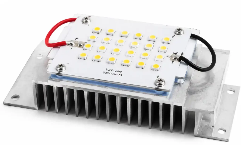
High-power LED applications demand efficient thermal management to maintain performance, color stability, and long-term reliability. Metal Core PCB (MCPCB) technology addresses this challenge by integrating a thermally conductive metal substrate directly into the circuit board structure, enabling rapid heat dissipation that standard FR4 boards cannot achieve. For LED design engineers working on street lighting, automotive headlamps, industrial high-bay fixtures, or architectural lighting systems, understanding MCPCB design rules and material selection is critical to preventing premature LED failure and maintaining lumen output over the product’s lifetime.
Table of Contents
- Why thermal management matters for high-power LED modules
- MCPCB construction and thermal conduction mechanism
- Material selection: aluminum vs copper core substrates
- Critical design rules for MCPCB LED applications
- MCPCB vs standard FR4: performance comparison for LED thermal management
- DFM considerations and common MCPCB fabrication pitfalls
- FAQ
- Conclusion and thermal design recommendations
1. Why thermal management matters for high-power LED modules
LED junction temperature directly controls luminous efficacy, color rendering index stability, and operational lifespan. For every 10°C increase in junction temperature above the rated maximum, LED lifespan typically decreases by 30-50%, and lumen depreciation accelerates. High-power LEDs operating at 1W to 10W per chip generate significant heat flux densities—often exceeding 50 W/cm²—that must be conducted away from the junction through the PCB substrate to an external heatsink.
Standard FR4 PCBs have thermal conductivity values of only 0.3-0.4 W/mK, creating a thermal bottleneck between the LED and the heatsink interface. This limitation forces thermal engineers to rely heavily on copper area and via stitching for heat spreading, which becomes impractical when board space is constrained or when LED arrays require high component density. MCPCB technology replaces the FR4 core with a metal substrate—typically aluminum or copper—offering thermal conductivity ranging from 1.0 to 8.0 W/mK depending on the dielectric layer specification. This fundamental material change enables direct thermal conduction through the board thickness rather than relying solely on lateral copper spreading.
For outdoor LED street lighting operating in ambient temperatures of 40-50°C, or automotive LED headlamps subjected to underhood temperatures exceeding 85°C, the thermal resistance from junction to heatsink becomes the limiting factor in LED drive current and luminous output. MCPCB reduces this thermal resistance path by 40-60% compared to equivalent FR4 designs, allowing higher LED drive currents, tighter LED spacing, and more compact luminaire designs without exceeding the LED manufacturer’s maximum junction temperature specification of 125-150°C.
2. MCPCB construction and thermal conduction mechanism
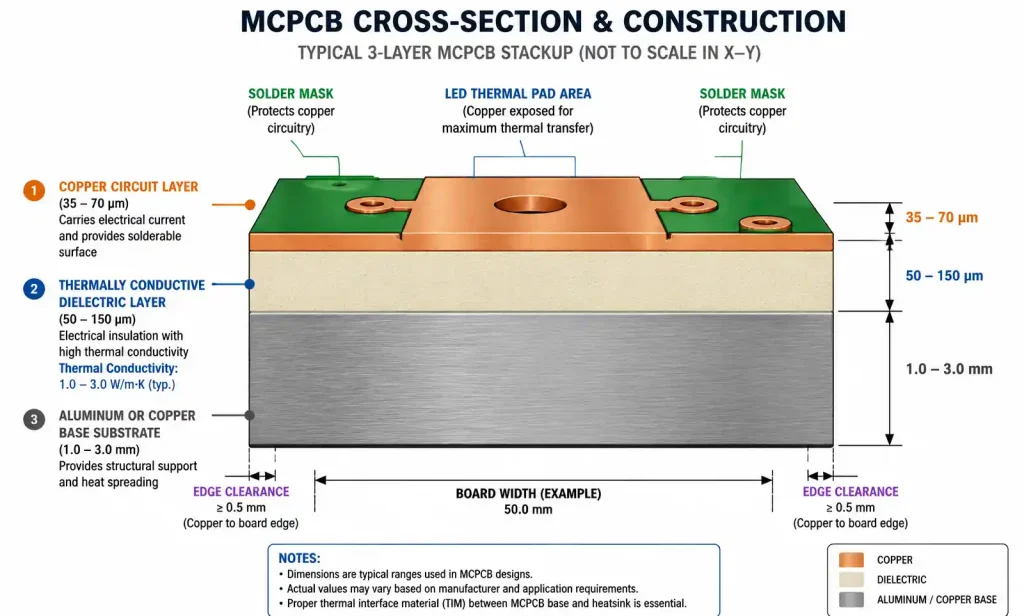
MCPCB consists of three primary layers: the metal base substrate, a thermally conductive dielectric layer, and the copper circuit layer. The metal base—most commonly aluminum alloy 5052 or 6061 with thickness ranging from 1.0mm to 3.0mm—serves as both the mechanical carrier and the primary thermal conduction path. Unlike FR4 laminates where the core material provides electrical insulation but poor thermal performance, the MCPCB dielectric layer must simultaneously achieve high dielectric breakdown strength (typically 3000V minimum) and high thermal conductivity (1.0 to 8.0 W/mK).
The dielectric layer, typically 50-150 microns thick, is composed of epoxy resin filled with ceramic particles such as aluminum oxide or boron nitride. The thermal conductivity of this dielectric layer determines the overall thermal performance of the MCPCB. Standard dielectric formulations offer 1.0-2.0 W/mK, suitable for LEDs up to 3W per chip. High-performance dielectrics using advanced ceramic fillers can achieve 3.0-4.0 W/mK for mid-power applications, while premium formulations reach 6.0-8.0 W/mK for ultra-high-power LED arrays exceeding 5W per chip.
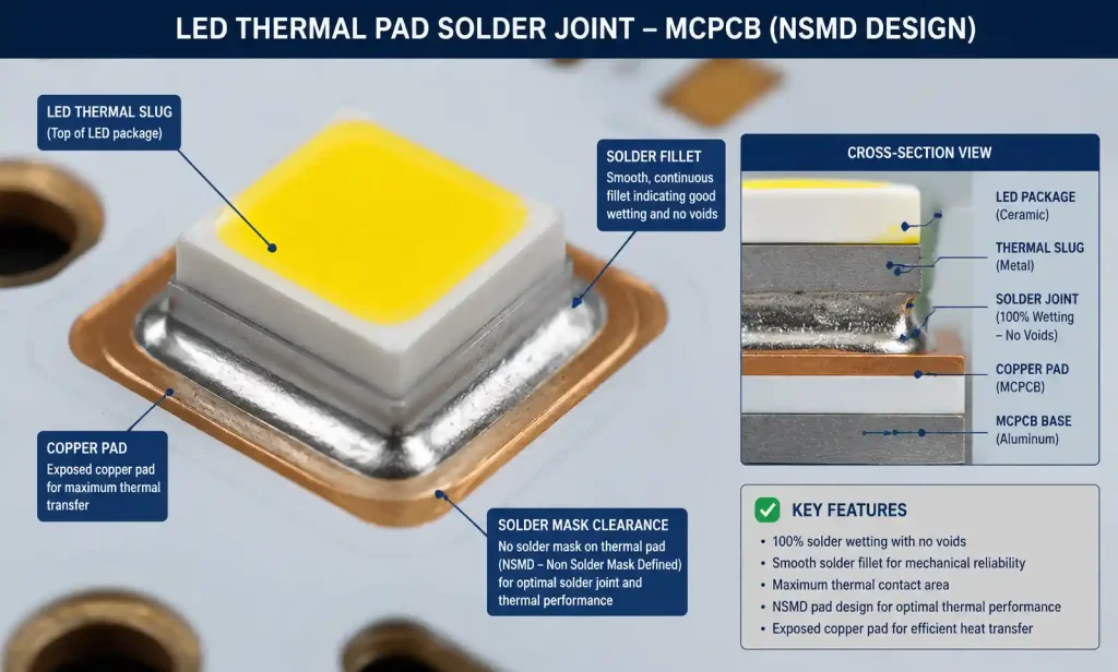
The copper circuit layer, typically 1oz (35μm) or 2oz (70μm), is bonded to the dielectric using thermal lamination processes. Heavier copper weights—3oz or 4oz—are sometimes specified for high-current LED driver circuits, but the thermal benefit is marginal since the metal base already provides the primary conduction path. The critical thermal interface is between the LED thermal pad and the copper circuit layer, which must be designed with maximum contact area and minimal thermal interface material (TIM) thickness.
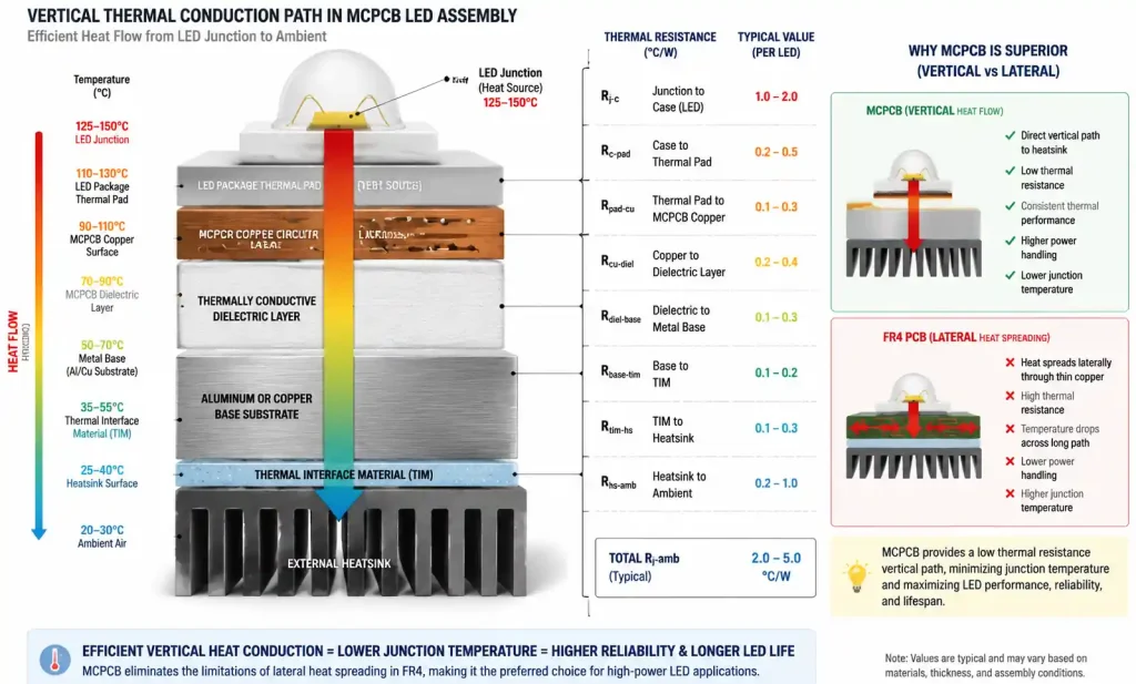
During operation, heat generated at the LED junction conducts through the LED package thermal pad into the MCPCB copper circuit layer. From there, heat flows vertically through the thin dielectric layer into the metal base substrate, which acts as an integrated heatsink. The metal base is then thermally coupled to an external heatsink using thermal grease or thermal adhesive tape, completing the thermal path from junction to ambient. This vertical conduction path through the MCPCB is significantly shorter and lower resistance than the lateral spreading path required in FR4 designs.
3. Material selection: aluminum vs copper core substrates
Aluminum and copper represent the two standard options for MCPCB base material, each with distinct thermal, mechanical, and cost trade-offs. Aluminum alloy 5052 offers thermal conductivity of approximately 200 W/mK, excellent formability, and low material cost, making it the dominant choice for cost-sensitive LED applications such as commercial lighting, residential downlights, and consumer electronics. The aluminum base is lightweight, corrosion-resistant, and easily machined for mounting holes and heatsink attachment features.
| Property | Aluminum 5052 Core | Copper Core | FR4 (Reference) |
|---|---|---|---|
| Thermal conductivity (W/mK) | 200 | 390 | 0.3-0.4 |
| Density (g/cm³) | 2.68 | 8.96 | 1.85 |
| CTE (ppm/°C) | 23.8 | 17.0 | 15-18 |
| Relative cost | 1.0x | 3.5-4.5x | 0.3x |
| Typical thickness (mm) | 1.0, 1.5, 2.0, 3.0 | 0.8, 1.0, 1.5, 2.0 | 0.8, 1.0, 1.6 |
| Weight (relative) | Medium | High | Low |
| Machinability | Excellent | Good | Poor |
Copper core MCPCB offers nearly double the thermal conductivity of aluminum at 390 W/mK, providing maximum thermal performance for ultra-high-power LED applications where junction temperature must be minimized. Copper’s higher density and cost limit its use to specialized applications such as LED surgical lighting, high-intensity stadium lighting, and aerospace LED indicators where thermal performance justifies the premium. Copper core also provides better CTE matching to ceramic LED packages, reducing thermomechanical stress during thermal cycling.
The dielectric layer material selection has equal or greater impact on overall thermal performance than base metal choice. A standard 2.0 W/mK dielectric on aluminum core typically outperforms a 1.0 W/mK dielectric on copper core for LED applications, because the dielectric layer represents the primary thermal bottleneck. When specifying MCPCB for high-power LEDs exceeding 3W per chip, prioritize dielectric thermal conductivity first, then consider base metal selection based on weight, cost, and secondary thermal performance requirements.
For automotive LED applications, aluminum core with 2.0-3.0 W/mK dielectric provides the best balance of thermal performance, weight, and vibration resistance. For architectural lighting where the MCPCB is directly visible or forms part of the luminaire housing, aluminum core with anodized or white solder mask finish offers aesthetic and thermal benefits. For ultra-compact LED modules with severe space constraints, copper core with high-conductivity dielectric minimizes the required heatsink volume.
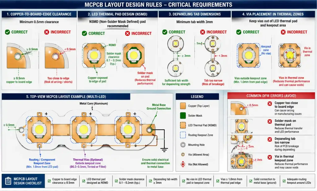
4. Critical design rules for MCPCB LED applications
LED thermal pad design directly determines the effectiveness of MCPCB thermal management. The LED thermal pad should be designed with maximum copper area, matching or exceeding the LED package thermal pad dimensions. Avoid solder mask on the LED thermal pad area; use NSMD (Non-Solder Mask Defined) pad design to maximize the direct thermal contact area between LED and copper. The copper pad should extend at least 0.5mm beyond the LED thermal pad on all sides to account for placement tolerance and ensure full solder joint formation.
Trace width and spacing for LED driver circuits must consider both current carrying capacity and thermal effects. For LED strings operating at 350mA to 1000mA, use minimum 0.3mm trace width for power distribution, increasing to 0.5-0.8mm for current paths exceeding 2A. Unlike FR4 designs where trace width calculations consider only copper thickness and temperature rise, MCPCB designs benefit from the enhanced heat sinking effect of the metal base. However, do not rely solely on this effect; maintain adequate trace width according to IPC-2152 current carrying capacity guidelines to prevent localized hot spots.
| Design Parameter | Standard LED (0.5-1W) | Mid-Power LED (1-3W) | High-Power LED (3-10W) |
|---|---|---|---|
| LED thermal pad copper | 1oz minimum | 2oz recommended | 2oz minimum |
| Thermal pad clearance to metal base | 0.3mm | 0.3mm | 0.4mm |
| Minimum trace width (power) | 0.25mm | 0.30mm | 0.40mm |
| Via diameter (if used) | 0.3mm | 0.4mm | Not recommended |
| Solder mask on thermal pad | No | No | No |
| Thermal interface material thickness | <50μm | <50μm | <30μm |
| Metal base thickness | 1.0-1.5mm | 1.5-2.0mm | 2.0-3.0mm |
Electrical clearance between the copper circuit layer and the metal base edge requires careful attention. The metal base is typically grounded for safety reasons, creating a conductive plane beneath the entire circuit. Maintain minimum 0.3mm clearance between any copper feature and the board edge to prevent electrical short during routing, depaneling, or heatsink mounting. For high-voltage LED drivers operating above 48VDC, increase this clearance to 0.5mm or greater according to IPC-2221 spacing requirements for your voltage class.
Thermal via usage in MCPCB designs differs fundamentally from FR4 thermal management strategies. In FR4 boards, thermal vias conduct heat from the component side to the backside copper pour, spreading heat laterally. In MCPCB, the metal base already provides superior heat spreading, making thermal vias redundant and potentially detrimental. Each via through the dielectric layer creates a potential thermal and electrical failure point. Avoid vias in the LED thermal pad area entirely. If vias are required for electrical routing, use minimum via count and ensure adequate annular ring on both sides.
5. MCPCB vs standard FR4: performance comparison for LED thermal management
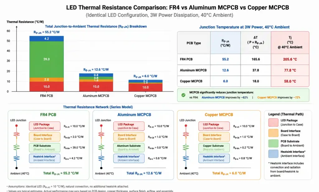
Thermal resistance from LED junction to ambient (Rθ-JA) serves as the key performance metric for comparing MCPCB and FR4 thermal management effectiveness. For a typical 3W LED with thermal pad dimensions of 7mm x 7mm, an FR4 board with 2oz copper and extensive thermal via array achieves Rθ-JA of approximately 25-30°C/W when mounted to a standard extruded aluminum heatsink. The same LED on MCPCB with 2.0 W/mK dielectric and identical heatsink achieves Rθ-JA of 12-15°C/W, reducing junction temperature by 30-45°C under identical drive current conditions.
This thermal resistance reduction translates directly to either extended LED lifespan at the same drive current, or increased lumen output by allowing higher drive current within the same junction temperature limit. For a 3W LED rated for 125°C maximum junction temperature, operating in 40°C ambient with 25°C/W thermal resistance limits the allowable power dissipation to 3.4W before exceeding the thermal limit. With 13°C/W thermal resistance using MCPCB, the same LED can safely dissipate 6.5W, enabling nearly double the luminous output from the same LED package.
| Thermal Performance Metric | FR4 (2oz Cu, Thermal Vias) | MCPCB (Al, 2.0 W/mK) | MCPCB (Cu, 4.0 W/mK) |
|---|---|---|---|
| Dielectric thermal conductivity | 0.3-0.4 W/mK | 2.0 W/mK | 4.0 W/mK |
| Rθ-Board (3W LED, 7x7mm pad) | 18-22°C/W | 5-7°C/W | 3-4°C/W |
| Rθ-JA (with heatsink) | 25-30°C/W | 12-15°C/W | 10-12°C/W |
| Junction temp at 3W, 40°C ambient | 115-130°C | 76-85°C | 70-76°C |
| Weight penalty vs FR4 | 1.0x | 1.8-2.2x | 4.0-5.0x |
| Typical lead time | 5-7 days | 7-10 days | 10-15 days |
| Relative cost (prototype) | 1.0x | 2.5-3.5x | 5.0-7.0x |
Cost and lead time represent the primary trade-offs when selecting MCPCB over FR4. For LED applications where thermal performance is not the limiting constraint—such as indicator LEDs, low-power accent lighting, or LEDs operating well below maximum rated current—standard FR4 remains the economical choice. However, for high-power LED applications where LED cost represents a significant portion of the BOM, MCPCB enables smaller LED packages, tighter LED spacing, and reduced heatsink volume, often resulting in lower total system cost despite higher PCB cost.
Manufacturing capability differences also influence the FR4 vs MCPCB decision. MCPCB fabrication requires specialized lamination equipment and typically supports simpler circuit designs. Minimum trace/space capabilities for MCPCB are generally 0.15/0.15mm to 0.20/0.20mm, adequate for LED power distribution but potentially limiting for integrated LED driver circuits with fine-pitch components. If your LED module design requires multilayer routing, blind/buried vias, or trace widths below 0.15mm, consider a hybrid approach using FR4 for the driver circuit and MCPCB for the LED mounting area, connected via board-to-board connectors or flex interconnect.
6. DFM considerations and common MCPCB fabrication pitfalls
MCPCB panelization and depaneling require different strategies than FR4 boards due to the metal substrate’s rigidity and thickness. V-scoring is not feasible for MCPCB; instead, use tab routing or full-cut separation. Design breakaway tabs with minimum 3mm width and include tooling holes for fixturing during depaneling. The metal base must be routed along with the dielectric and copper layers, requiring carbide end mills and slower cutting speeds. Plan for wider kerf width—typically 2.0-2.5mm compared to 1.5mm for FR4 routing—when calculating panel utilization.
The metal base edge exposure after routing creates a potential electrical hazard if not properly managed. Most MCPCB designs require an insulating coating applied to the board edge, either during fabrication or as a post-assembly process. Alternatively, design the copper circuit layer with adequate setback from the board edge—minimum 0.5mm—to ensure no copper overhangs the metal base after routing. For LED modules mounted directly into conductive heatsink housings, this edge clearance prevents accidental short circuits between the circuit layer and grounded metal parts.
Solder mask application on MCPCB follows different process parameters than FR4 due to the metal base’s high thermal mass and CTE mismatch with the organic solder mask material. White solder mask is common for LED applications to enhance light reflection, but requires thicker application and longer cure times than standard green mask. Ensure your MCPCB manufacturer has experience with white mask on metal core substrates, as adhesion failures and cracking during thermal cycling are common DFM issues. Specify solder mask thickness of 15-25 microns minimum to ensure adequate dielectric protection and UV reflectivity.
Component placement constraints on MCPCB differ from FR4 designs due to the reduced board flexibility and higher thermal mass during reflow. Heavy components should be oriented with their mass centroid centered over the board area, not cantilevered over the edge, to prevent board warpage during reflow. SMT component packages with large thermal pads—such as power MOSFETs, driver ICs, or high-current inductors—require careful reflow profile optimization. The metal base acts as a heat sink during reflow, potentially creating temperature gradients across the board that can cause tombstoning or non-wetting. Use zone heating or selective preheating to compensate for the metal base thermal mass.
| DFM Check Item | Requirement | Risk if Not Met | Recommended Action |
|---|---|---|---|
| Copper to board edge clearance | ≥0.5mm | Electrical short during mounting | Increase clearance or add edge insulation coating |
| Tab width for depaneling | ≥3.0mm | Board fracture during separation | Use wider tabs or mouse-bites |
| Solder mask on thermal pads | None | Acceptable thermal interface | Set NSMD for all LED pads |
| Via in LED thermal pad area | None (avoid) | Solder void, thermal resistance | Route without vias under LEDs |
| Reflow profile validation | Required | Cold solder joints, tombstoning | Test with metal core dummy board first |
| Metal base grounding | Specify clearly | Safety hazard, EMI issues | Add GND connection point or isolate |
Thermal interface material application between the MCPCB metal base and the external heatsink critically affects overall thermal performance. Even small air gaps of 50-100 microns can add 2-5°C/W thermal resistance, negating much of the MCPCB benefit. Specify thermal grease with thermal conductivity above 3.0 W/mK and apply with controlled bondline thickness using fixturing or measured torque on mounting screws. Thermal adhesive tapes offer consistent bondline thickness and simplified assembly but typically have lower thermal conductivity (1.5-2.5 W/mK). For high-volume production, automated thermal grease dispensing ensures consistent application thickness and minimizes thermal resistance variation unit-to-unit.
7. FAQ
What is the typical thermal conductivity range for MCPCB dielectric layers used in LED applications?
Standard MCPCB dielectric layers offer 1.0-2.0 W/mK, suitable for LEDs up to 3W per chip. High-performance dielectrics range from 3.0-4.0 W/mK for mid-power applications, while premium formulations reach 6.0-8.0 W/mK for ultra-high-power LED arrays. The dielectric layer thermal conductivity has greater impact on overall thermal performance than the base metal choice.
Can I use thermal vias in MCPCB LED designs like I do with FR4 boards?
No. Thermal vias are generally not recommended in MCPCB designs because the metal base already provides superior heat spreading. Each via through the dielectric creates a potential failure point and adds minimal thermal benefit. Avoid vias entirely in LED thermal pad areas, and minimize via count elsewhere for electrical routing.
How do I calculate the required metal base thickness for my LED application?
Metal base thickness selection depends on LED power level, mounting configuration, and mechanical requirements. For LEDs under 3W, use 1.0-1.5mm thickness. For 3-10W LEDs, specify 1.5-2.0mm. For ultra-high-power arrays or applications requiring structural rigidity, use 2.0-3.0mm. Thicker bases provide better heat spreading but increase weight and material cost.
What surface finish should I specify for the LED thermal pads on MCPCB?
ENIG (Electroless Nickel Immersion Gold) is the preferred surface finish for LED thermal pads, providing excellent solderability, flat surface for optimal thermal contact, and long shelf life. Avoid HASL (Hot Air Solder Leveling) due to uneven surface topology that increases thermal interface resistance. Immersion silver is an economical alternative with good thermal performance but shorter shelf life.
Why is white solder mask commonly used on LED MCPCB designs?
White solder mask enhances light reflection and increases luminaire efficiency by reflecting stray LED light back toward the intended light output direction. White mask also improves visual inspection of solder joints during assembly and reflects heat, slightly reducing LED junction temperature. However, white mask requires thicker application and careful process control to prevent cracking.
Can MCPCB be used for multilayer circuit designs with blind or buried vias?
Standard MCPCB is a single-layer circuit technology—copper on one side of a metal core. Some manufacturers offer two-layer MCPCB with circuitry on both sides of the metal base, separated by dielectric layers. However, multilayer routing with buried vias is not feasible. For complex LED driver circuits, consider hybrid designs with separate FR4 multilayer boards connected to MCPCB LED mounting areas.
What is the expected lead time difference between FR4 and MCPCB prototype orders?
Standard FR4 prototypes typically ship in 5-7 days from major PCB manufacturers. MCPCB prototypes require 7-10 days due to specialized lamination processes and material procurement. High-conductivity dielectric formulations (>3.0 W/mK) may extend lead time to 10-15 days. Plan accordingly when scheduling LED module development timelines.
How should I specify the metal base grounding for safety compliance?
The metal base should be electrically grounded to the system ground reference to prevent electrical shock hazard and reduce EMI. Provide at least one dedicated grounding pad connected to the circuit layer ground plane and specify that the MCPCB manufacturer electrically connect this pad to the metal base. Include this grounding requirement clearly in your fabrication drawing notes.
8. Conclusion and thermal design recommendations
MCPCB technology fundamentally changes the thermal management equation for high-power LED modules by providing a low-resistance thermal conduction path directly through the board substrate. For LED applications operating above 2W per chip, or where junction temperature control is critical to lifespan and performance, MCPCB offers 40-60% reduction in thermal resistance compared to FR4 designs, enabling higher drive currents, tighter LED spacing, and more compact luminaire designs.
When specifying MCPCB for your LED application, prioritize dielectric layer thermal conductivity first—2.0 W/mK as a baseline for mid-power LEDs, 3.0-4.0 W/mK for high-power applications. Aluminum core provides the best balance of thermal performance, weight, and cost for most LED lighting applications. Reserve copper core for specialized applications where maximum thermal performance justifies the cost and weight penalty. Design LED thermal pads with maximum copper area, avoid vias in thermal zones, and maintain adequate clearance between circuit features and the metal base edge to ensure manufacturable, reliable designs.
Before committing to volume production, validate your MCPCB thermal design with prototype builds and thermal testing under worst-case operating conditions. Measure LED junction temperature using forward voltage method or thermal imaging to confirm that thermal resistance meets your design targets. If junction temperature exceeds expectations, investigate thermal interface material application quality, heatsink contact pressure, and LED thermal pad solder joint formation before redesigning the MCPCB stackup.
For design review assistance or questions about MCPCB material selection, dielectric thermal conductivity options, or DFM optimization for your LED application, contact our CAM engineering team. We offer free thermal design analysis and can recommend the optimal MCPCB stackup for your specific LED power level, operating environment, and cost targets.