8 Layer PCB with Via-in-Pad: When and Why to Use This Technology
Via-in-pad technology has become a critical design technique for 8-layer PCB layouts, especially when routing high-density BGA components, DDR memory interfaces, and high-speed differential pairs. This guide explains when via-in-pad is necessary, why it outperforms traditional via routing in specific scenarios, and what design rules and manufacturing considerations you need to follow to ensure reliable production.
Table of Contents
- Introduction: What This Guide Covers
- Understanding Via-in-Pad Technology in 8-Layer PCBs
- When to Use Via-in-Pad: Critical Design Scenarios
- Why Via-in-Pad Matters: Technical Benefits and Trade-offs
- Design Rules and Manufacturing Considerations
- Via-in-Pad vs Traditional Via Routing: Comparison
- FAQ
- Conclusion and Design Recommendations
1. Introduction: What This Guide Covers
When designing high-density 8-layer PCBs with fine-pitch BGAs, you quickly run into a routing bottleneck: there simply isn’t enough space between pads to place vias for escape routing using traditional design rules. Via-in-pad technology solves this problem by placing vias directly within the component pad, allowing signal traces to transition between layers without consuming valuable routing channels.
This guide is written for PCB layout engineers, hardware design engineers, and manufacturing engineers who need to make informed decisions about via-in-pad implementation. You’ll learn the specific design scenarios where via-in-pad is necessary, the manufacturing processes required to ensure reliability, and the cost and DFM trade-offs involved. By the end of this article, you’ll understand when via-in-pad justifies its additional manufacturing cost and how to specify it correctly in your fabrication documentation.
The focus is on 8-layer stackups because this layer count provides sufficient routing layers for complex designs while remaining cost-effective for volume production. Via-in-pad becomes particularly relevant in 8-layer boards when component density increases or when controlled impedance requirements demand tighter routing discipline.
2. Understanding Via-in-Pad Technology in 8-Layer PCBs
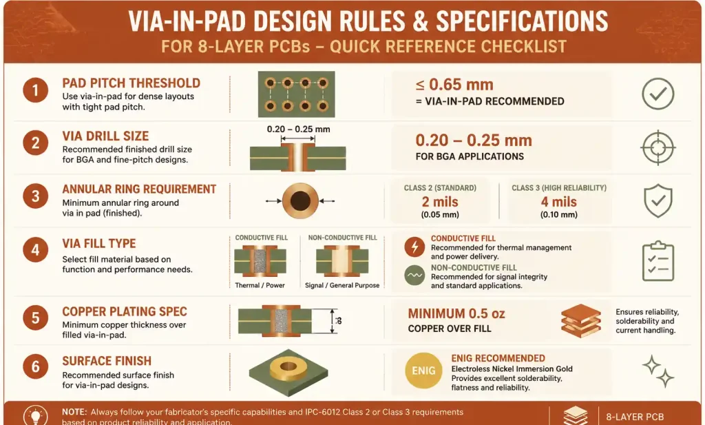
Via-in-pad refers to the practice of placing a plated through-hole or microvia directly inside a surface-mount component pad. In standard PCB design, vias are offset from pads to prevent solder wicking down the via barrel during reflow, which can cause poor solder joints, voiding, or component misalignment. However, when pad pitch drops below 0.65mm or when routing density becomes extreme, offsetting vias is no longer geometrically feasible.
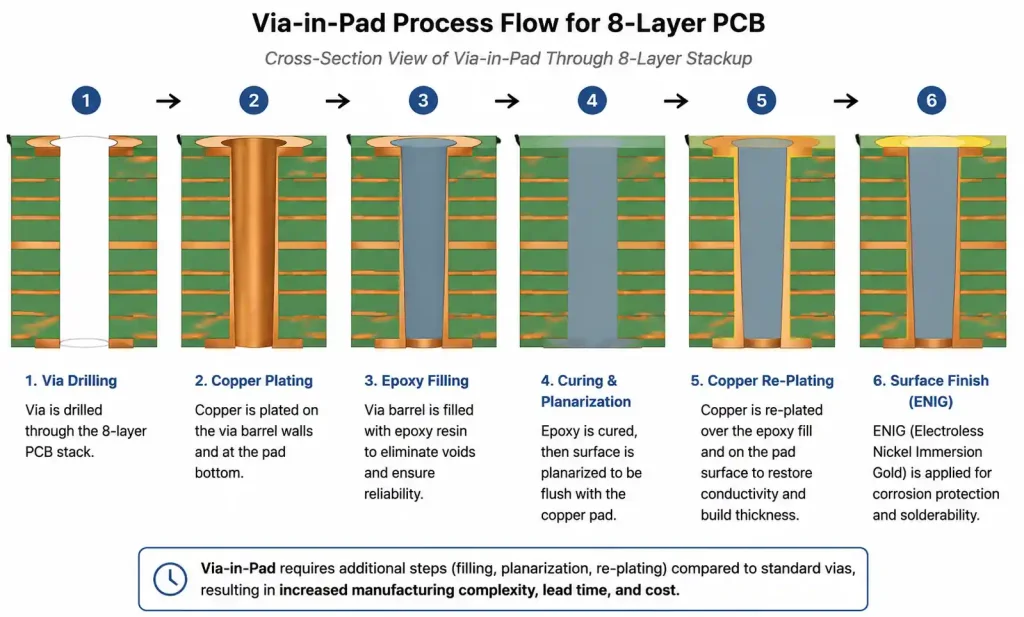
To make via-in-pad reliable for assembly, the via must be filled and plated over. The manufacturing process typically involves drilling and plating the via, filling it with conductive or non-conductive epoxy, then copper-plating over the filled via to create a flat, solderable surface. This prevents solder from wicking into the barrel and ensures a consistent solder joint formation during reflow.
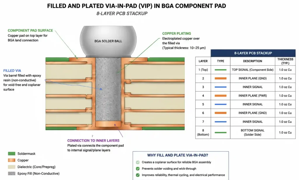
In an 8-layer PCB, via-in-pad is most commonly applied to high-pin-count components such as BGAs, QFNs, and LGAs. These components often have pad pitches of 0.5mm or finer, leaving no room for traditional via fanout. For example, a 0.5mm pitch BGA may have pads with a diameter of 0.275mm and a pad-to-pad clearance of only 0.225mm. Placing a 0.2mm via between pads would violate minimum solder mask dam requirements and create severe DFM risks.
The stackup design for an 8-layer board using via-in-pad should account for controlled impedance on inner signal layers and sufficient copper distribution to support via plating uniformity. A typical 8-layer stackup for via-in-pad applications might be: Top Layer (signal) / GND / Signal / Signal / GND / PWR / Signal / Bottom Layer (signal), with via transitions occurring primarily between the top layer and inner signal layers.
3. When to Use Via-in-Pad: Critical Design Scenarios
Via-in-pad is not a default choice for every 8-layer design. It introduces additional manufacturing cost, longer lead times, and stricter DFM requirements. You should consider via-in-pad when one or more of the following conditions apply.
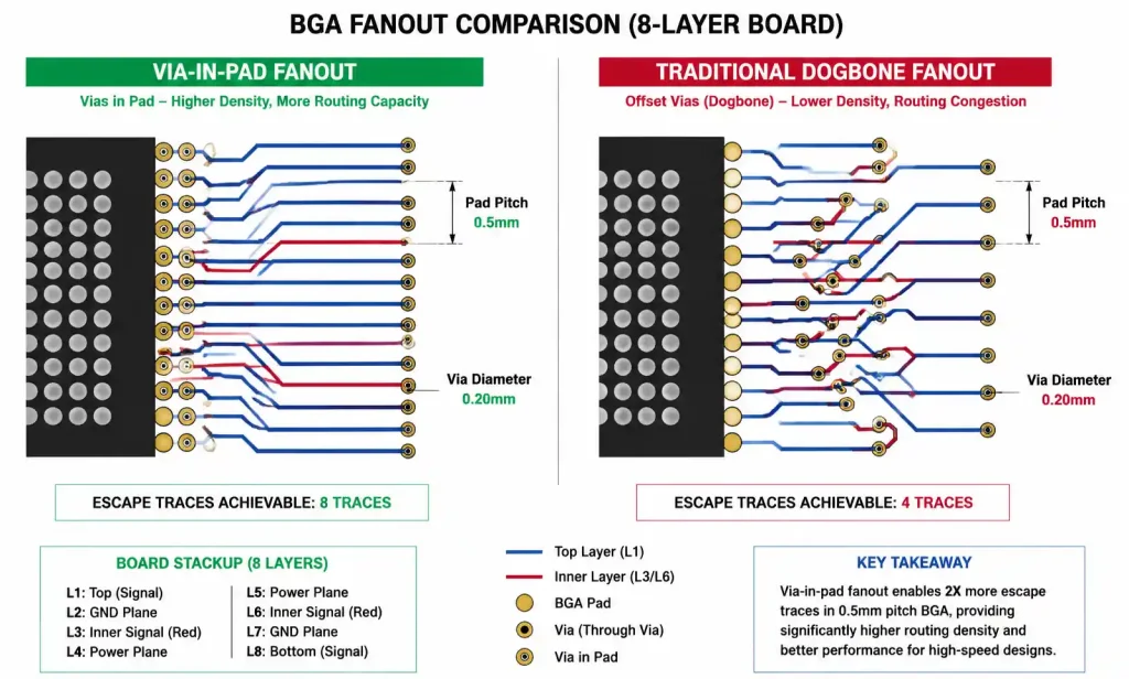
Fine-pitch BGA components with pad pitch ≤ 0.65mm. For BGA packages with 0.5mm or 0.4mm pitch, there is insufficient space between pads to place breakout vias using IPC-2221 or IPC-7351 guidelines. Attempting to squeeze vias between pads results in solder mask slivers below 4 mils, which increases the risk of solder bridging and mask delamination. Via-in-pad allows each pad to support a direct vertical transition without lateral routing congestion.
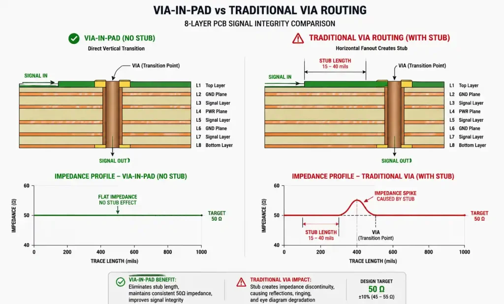
High-speed differential pairs requiring length matching and impedance control. When routing USB 3.0, PCIe, HDMI, or DDR4 interfaces on an 8-layer board, length matching tolerances can be as tight as ±5 mils. Traditional dogbone fanout adds 20–40 mils per via pair, making it difficult to meet timing budgets. Via-in-pad eliminates the fanout trace, shortening signal paths and reducing impedance discontinuities caused by stub length.
Dense power delivery networks with multiple voltage rails. Modern FPGAs, SoCs, and high-performance processors require multiple power domains (e.g., 1.0V, 1.8V, 3.3V) with dedicated decoupling capacitors placed as close as possible to the IC. When decoupling capacitors are placed on the bottom side directly under the BGA, via-in-pad allows power and ground vias to connect through the capacitor pads without detouring around them, reducing PDN inductance.
Thermal management in high-power applications. For power semiconductors, RF amplifiers, or LED drivers on an 8-layer board, via-in-pad under thermal pads or exposed die-attach pads improves thermal conductivity to inner ground planes. Filled and plated vias provide a lower thermal resistance path compared to open vias, which trap air and reduce heat transfer efficiency.
4. Why Via-in-Pad Matters: Technical Benefits and Trade-offs
Via-in-pad offers several technical advantages that directly impact signal integrity, thermal performance, and routing efficiency. However, these benefits come with increased manufacturing complexity and cost.
Signal integrity improvement. Traditional via fanout introduces a trace stub between the component pad and the via, creating an impedance discontinuity that reflects high-frequency signals. For signals above 1 GHz, stub length should be kept below 10 mils to avoid resonance and return loss degradation. Via-in-pad eliminates the stub entirely, providing a cleaner impedance profile and better eye diagram performance at the receiver. This is especially critical for SerDes interfaces like 10 Gbps Ethernet or PCIe Gen 3, where signal rise times are below 50 picoseconds.
Routing density increase. By placing vias inside pads, you free up the inter-pad space for signal routing. On an 8-layer board with a fine-pitch BGA, this can double the number of available routing channels in the breakout region. For example, a 0.5mm pitch BGA with via-in-pad allows four or more traces to escape between adjacent rows, compared to only one or two traces with traditional fanout.
Thermal conductivity enhancement. When vias are filled with conductive epoxy and copper-plated, they act as vertical thermal conduits. A 0.3mm via filled with copper-loaded epoxy can reduce thermal resistance by 30–40% compared to an open via. For high-current applications like DC-DC converters or motor drivers, this thermal improvement can lower junction temperature by 10–15°C, improving reliability and reducing the need for external heatsinks.
Manufacturing cost and lead time. The primary trade-off is cost. Via-in-pad requires via filling, planarization, and additional copper plating, adding 15–30% to the bare PCB fabrication cost depending on board complexity and order volume. Lead time increases by 2–4 days for prototype runs. Additionally, via fill quality must meet IPC-4761 Type VII or Type VIII requirements to ensure a planar surface suitable for fine-pitch assembly. Not all PCB manufacturers support via-in-pad, so supplier selection becomes more critical.
DFM risk factors. Via-in-pad introduces several manufacturability challenges: incomplete via fill causing voids, non-planar via caps leading to solder joint defects, copper plating thickness variation across the board, and differential thermal expansion between the via fill material and the surrounding copper. These risks are mitigated through proper material selection, process control, and incoming inspection, but they require tighter collaboration between design, CAM, and manufacturing teams.
5. Design Rules and Manufacturing Considerations
To ensure reliable via-in-pad implementation on an 8-layer PCB, you must follow specific design rules and clearly communicate requirements to your fabrication house.
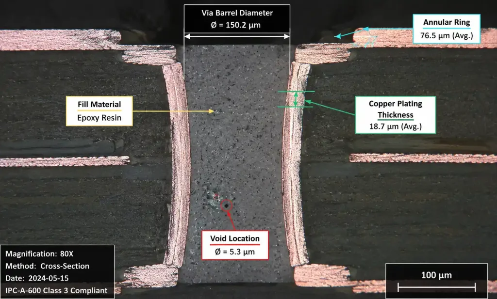
Via size and fill specifications. For BGAs with pad diameters between 0.25mm and 0.35mm, the via drill size should be 0.2mm to 0.25mm. The finished via diameter after plating will be approximately 0.15mm to 0.2mm. Specify via fill material in your fabrication notes: conductive epoxy for thermal vias under power components, non-conductive epoxy for signal vias where electrical isolation from the barrel is needed. The via fill must be planar within ±1 mil of the surrounding pad surface to prevent solder joint defects.
Copper plating over filled vias. After filling, the via must be copper-plated to restore electrical continuity and provide a solderable surface. Specify a minimum of 0.5 oz (18 µm) copper plating over the filled via. This plating must match the surface finish applied to the rest of the board (ENIG, ENEPIG, or Immersion Silver). Some manufacturers apply the surface finish before via filling, which can cause adhesion issues; verify the process sequence with your fabricator.
Pad size and annular ring requirements. For via-in-pad, the component pad diameter must be at least 0.05mm larger than the via drill diameter to ensure a minimum 0.025mm (1 mil) annular ring around the via. This annular ring is necessary for via plating integrity and to prevent via blowout during drilling. For IPC Class 2 designs, a 2 mil annular ring is acceptable; for IPC Class 3 (aerospace, medical), increase to 4 mils.
| IPC Class | Minimum Annular Ring | Recommended Pad Diameter (for 0.2mm via) | Via Fill Type | Plating Over Fill |
|---|---|---|---|---|
| Class 2 (Consumer) | 2 mils (0.05mm) | 0.30mm | Non-conductive epoxy | 0.5 oz Cu + ENIG |
| Class 3 (High reliability) | 4 mils (0.1mm) | 0.35mm | Conductive epoxy | 1 oz Cu + ENIG |
| Thermal via (Power) | 2 mils (0.05mm) | 0.35mm | Conductive epoxy | 0.5 oz Cu + ENIG |
This table shows the relationship between IPC class requirements, via geometry, and manufacturing specifications. For high-reliability designs, the larger annular ring provides additional margin against registration errors during drilling and plating. Thermal vias benefit from conductive fill to maximize heat transfer, while signal vias typically use non-conductive fill to avoid unintended ground coupling.
Solder mask treatment. Via-in-pad areas should be defined as solder mask-defined pads (SMD) rather than non-solder mask-defined pads (NSMD) when pad diameter exceeds 0.4mm. For smaller pads, NSMD is preferred to maximize the solderable area. Ensure solder mask dams between adjacent pads are at least 4 mils wide; if this is not achievable, consider gang masking or requesting a solder mask registration tolerance analysis from your fabricator.
Acceptance criteria and inspection. Specify IPC-A-600 Class 2 or Class 3 acceptance criteria in your fabrication drawing. For via-in-pad, key inspection points include: via fill void content (should be < 10% by volume for Class 3), surface planarity (measured by profilometry or cross-section), copper thickness over fill (measured by microsection), and solder joint quality after assembly (evaluated by X-ray inspection). Request a first article inspection (FAI) report for new designs to verify via fill integrity before committing to volume production.
6. Via-in-Pad vs Traditional Via Routing: Comparison
The decision between via-in-pad and traditional via routing depends on component pitch, signal speed, routing density, and budget constraints. The table below compares these approaches across key design and manufacturing dimensions.
| Parameter | Via-in-Pad | Traditional Via Routing (Dogbone Fanout) |
|---|---|---|
| Suitable pad pitch | ≤ 0.65mm | ≥ 0.8mm |
| Signal stub length | 0 mils (via directly in pad) | 15–40 mils (fanout trace + via) |
| Routing channels saved | +50% to +100% in breakout region | Baseline |
| Impedance discontinuity | Minimal (no stub resonance) | Moderate (stub causes reflection) |
| Thermal resistance (per via) | 0.8–1.2 °C/W (with conductive fill) | 1.5–2.5 °C/W (open via) |
| Fabrication cost increase | +15% to +30% | Baseline |
| Lead time increase | +2 to +4 days (prototype) | Baseline |
| Manufacturing complexity | High (via fill, planarization, plating) | Low (standard process) |
| DFM risk | Moderate (void formation, planarity) | Low |
| IPC-A-600 Class 3 yield | 95–98% (with experienced fab house) | 98–99% |
This comparison highlights the trade-off between routing efficiency and manufacturing cost. Via-in-pad is justified when pad pitch or signal integrity requirements make traditional routing infeasible. For 8-layer boards with 0.5mm pitch BGAs and multi-gigabit interfaces, the cost premium is offset by the ability to route the design successfully without moving to 10 or 12 layers.
When routing density is not a limiting factor, traditional via fanout remains the more cost-effective and manufacturable option. For example, a 0.8mm pitch BGA on an 8-layer board can be routed with dogbone fanout without compromising signal integrity, and the fabrication cost will be 15–20% lower. Always evaluate the minimum viable approach before specifying via-in-pad.
7. FAQ
What is the minimum pad size for via-in-pad on an 8-layer PCB?
The minimum pad size depends on the via drill diameter and the required annular ring. For a 0.2mm via drill, the minimum pad diameter is 0.30mm for IPC Class 2 (allowing a 2 mil annular ring) and 0.35mm for IPC Class 3 (allowing a 4 mil annular ring). Pads smaller than 0.25mm are generally not suitable for via-in-pad due to insufficient annular ring and increased risk of via blowout during drilling.
Can I use via-in-pad for both signal and power/ground connections?
Yes, via-in-pad works for both signal and power/ground vias, but the via fill material should differ. For signal vias, non-conductive epoxy is preferred to avoid unintended coupling to ground planes. For power and ground vias, conductive epoxy maximizes current-carrying capacity and thermal conductivity. Clearly specify via fill type in your fabrication notes, and consider using different via drill sizes to help the fabricator distinguish between signal and power vias during processing.
Does via-in-pad require a specific surface finish?
Via-in-pad is compatible with ENIG, ENEPIG, Immersion Silver, and OSP surface finishes. ENIG is the most common choice for fine-pitch BGAs because it provides a flat, solderable surface and excellent shelf life. OSP is lower cost but offers a shorter shelf life and may not adhere well to epoxy-filled vias if the surface is not properly prepared. Avoid HASL (hot air solder leveling) for via-in-pad because the uneven solder coating can create planarity issues and cause solder joint defects.
How much does via-in-pad add to PCB fabrication cost?
Via-in-pad typically adds 15–30% to the bare board cost, depending on the number of vias to be filled, the total board area, and the fabricator’s process capability. For a prototype run of 10 boards, expect an additional $100–$300. For volume production (500+ boards), the cost premium decreases to 10–15% as the via fill process is amortized over a larger quantity. Always request a detailed quote that separates via fill charges from base fabrication cost.
What are common defects associated with via-in-pad?
The most common defects are void formation inside the filled via, non-planar via caps (causing solder starvation or tombstoning), and delamination between the via fill material and the copper barrel. Voids occur when the epoxy is not fully degassed before filling or when the via aspect ratio is too high. Non-planar caps result from insufficient planarization after filling. Delamination is caused by CTE mismatch between the fill material and the PCB substrate, especially during thermal cycling. To minimize these risks, work with a fabricator experienced in via-in-pad processing and request cross-sectional analysis for first article inspection.
Can I mix via-in-pad and traditional via routing on the same board?
Yes, this is a common practice. Use via-in-pad only where necessary (e.g., under fine-pitch BGAs or in high-density routing regions) and use traditional via routing elsewhere to minimize cost. Clearly mark via-in-pad areas in your fabrication drawing using a unique via designation (e.g., “VIP” in the via net name) so the fabricator knows which vias require filling and plating. This hybrid approach balances manufacturability and cost while meeting design requirements.
What is the typical lead time for an 8-layer PCB with via-in-pad?
For prototype orders, expect 10–14 days for an 8-layer board with via-in-pad, compared to 7–10 days for a standard 8-layer board without via fill. Volume production lead times are typically 3–4 weeks. The via fill process adds 2–3 days due to the additional steps: drilling, plating, filling, curing, planarization, and re-plating. Expedited options may be available for an additional cost, but via fill quality can suffer if process steps are rushed.
How do I specify via-in-pad requirements in my Gerber files?
In your fabrication drawing, include a note specifying: “Vias marked VIP in drill file shall be filled with [conductive/non-conductive] epoxy, planarized, and copper-plated per IPC-4761 Type VII. Final surface must be planar within ±1 mil. Surface finish: ENIG, 3–5 µin gold over 120–240 µin nickel.” In your drill file, use a unique tool code or net name prefix (e.g., “VIP_”) to identify via-in-pad locations. Provide a cross-sectional drawing showing the expected via fill profile and plating thickness.
8. Conclusion and Design Recommendations
Via-in-pad is a specialized but essential technique for 8-layer PCB designs involving fine-pitch BGAs, high-speed interfaces, or dense power delivery networks. When pad pitch drops below 0.65mm or when signal integrity constraints demand minimal stub length, via-in-pad becomes the only viable routing solution. The technology eliminates fanout traces, reduces impedance discontinuities, and increases routing density, but it requires careful attention to via fill quality, pad geometry, and manufacturing process control.
Before committing to via-in-pad, evaluate whether your design truly requires it. If traditional via routing can meet your electrical and routing requirements, it will save cost and reduce manufacturing risk. When via-in-pad is necessary, work closely with your PCB fabricator to ensure they have the process capability and experience to deliver reliable via fill. Request a first article inspection and cross-sectional analysis to verify via fill integrity before moving to volume production.
For your next 8-layer design, use this guide to determine whether via-in-pad is justified. If you’re routing a 0.5mm pitch BGA with DDR4 interfaces or PCIe lanes, via-in-pad will simplify your layout and improve signal quality. If your design uses larger pitch components and has adequate routing space, stick with traditional via fanout to minimize cost and lead time.
Need help evaluating your specific design scenario? Upload your layout files for a free DFM review, or use our online via-in-pad cost calculator to estimate fabrication impact. Our CAM engineering team can assess your via-in-pad requirements and recommend the optimal stackup and via fill specification for your application.