BGA 0.18mm Assembly: Challenges and Solutions for Ultra-Fine Pitch
Ultra-fine pitch BGA assembly represents one of the most demanding processes in modern electronics manufacturing. When ball pitch reaches 0.18mm, the margin for error becomes microscopic, and traditional assembly methods often prove inadequate. This guide explores the critical challenges assembly engineers face with 0.18mm pitch BGAs and provides proven solutions based on production-level manufacturing experience.
Table of Contents
- What Makes 0.18mm Pitch BGA Assembly Uniquely Challenging
- Critical Design and Layout Requirements
- PCB Manufacturing Tolerances and Stackup Considerations
- Assembly Process Requirements and Equipment Specifications
- Solder Paste and Reflow Profile Optimization
- X-ray Inspection and Quality Control Methods
- Common Defects and Troubleshooting Strategies
- FAQ
- Conclusion and Recommended Next Steps
1. What Makes 0.18mm Pitch BGA Assembly Uniquely Challenging
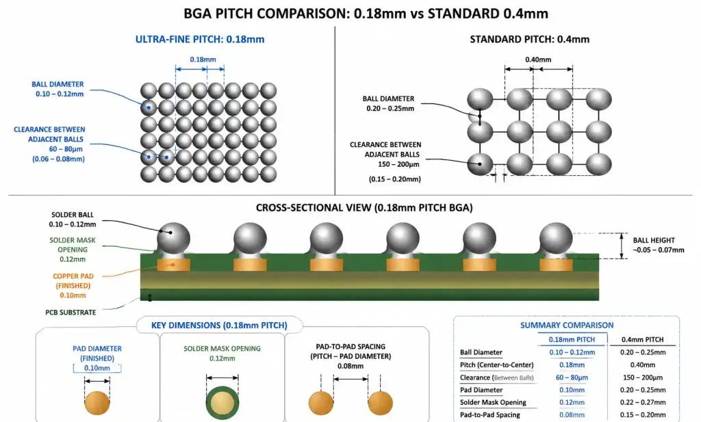
At 0.18mm ball pitch, we’re operating at the practical limits of conventional SMT assembly. The solder ball diameter typically measures between 0.10mm and 0.12mm, leaving only 60-80 microns of clearance between adjacent balls. This creates multiple compounding challenges that don’t exist at standard 0.4mm or 0.5mm pitch levels.
The primary challenge stems from pad-to-pad spacing. With 0.18mm pitch, the PCB pad diameter is typically 0.10mm with 0.08mm spacing between pads. Any registration error beyond ±25 microns can cause bridging or insufficient solder joint formation. Standard pick-and-place equipment specified for ±50 micron placement accuracy becomes marginal at this pitch.
Solder paste printing presents another critical constraint. Type 6 or Type 7 solder powder is required, with particle sizes of 15-25 microns for Type 6 and 10-20 microns for Type 7. The stencil aperture must be designed with extreme precision, typically requiring laser-cut stainless steel stencils with electropolished apertures. Nano-coated stencils help with paste release, but even minor variations in stencil thickness or aperture geometry can cause print defects.
Thermal management during reflow becomes significantly more complex. The reduced solder volume per joint means less thermal mass to buffer temperature variations. At the same time, the high ball count and density increase the risk of warpage-induced open joints. Components with 0.18mm pitch often have 500+ balls, and achieving uniform heating across the entire array requires precise process control.
X-ray inspection capability becomes mandatory rather than optional. Standard AOI cannot verify solder joint quality under the component. X-ray systems must provide sufficient resolution to detect voids, bridging, and incomplete wetting at 0.10mm ball diameter. Many standard X-ray systems lack the magnification and detector resolution needed for reliable inspection.
2. Critical Design and Layout Requirements
Successful 0.18mm pitch BGA assembly starts at the PCB design stage. The pad design must account for both manufacturing tolerances and assembly process requirements. Non-solder mask defined (NSMD) pads are essential for ultra-fine pitch applications.
For 0.18mm pitch BGAs, the recommended NSMD pad design uses a copper pad diameter of 0.10mm with solder mask opening of 0.12-0.13mm. This creates a 10-15 micron annular solder mask dam around each pad, which helps prevent bridging while maintaining sufficient solder wetting area. The solder mask registration tolerance must be held to ±25 microns or better.
| Design Parameter | 0.18mm Pitch Specification | 0.25mm Pitch (Reference) | Critical Factor |
|---|---|---|---|
| Copper pad diameter | 0.10mm | 0.15mm | Solder joint strength |
| Solder mask opening | 0.12-0.13mm | 0.17-0.18mm | Bridging prevention |
| Pad-to-pad clearance | 0.08mm | 0.10mm | Manufacturing yield |
| Via-in-pad diameter | 0.10mm max | 0.15mm max | Solder wicking risk |
| Via fill requirement | Copper-filled + plated | Copper-filled + plated | Joint reliability |
| Solder mask registration | ±25μm | ±50μm | Defect rate driver |
| PCB thickness tolerance | ±0.05mm | ±0.10mm | Placement accuracy |
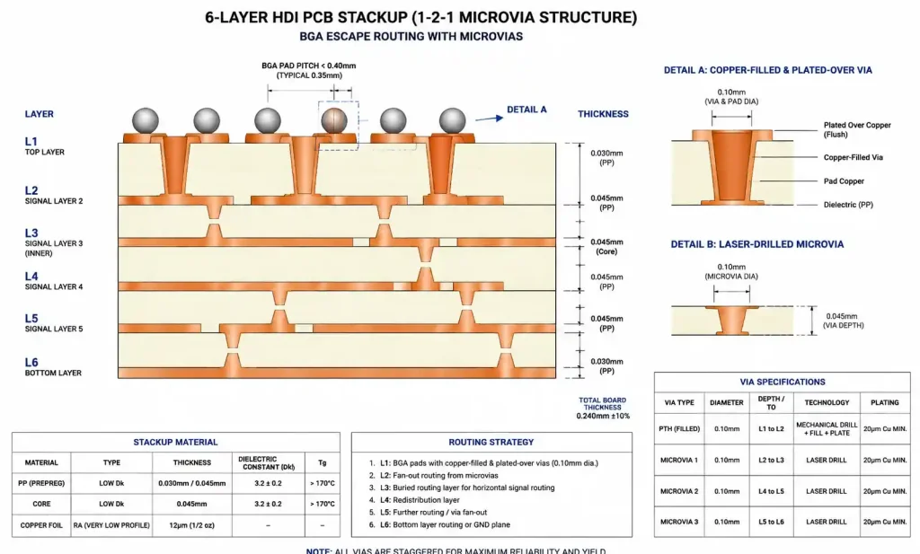
Via-in-pad design requires special attention. If routing density demands vias within the BGA pad footprint, those vias must be copper-filled and plated over. Partial via fill or tenting is insufficient at this pitch because solder wicking into even small via openings can starve the joint. The via diameter should not exceed 0.10mm, and the via should be centered within the pad.
Routing escape strategies must be planned carefully. With 0.08mm pad-to-pad spacing, there is no room to route traces between pads. All routing must escape via buried or blind vias, or through microvias if using HDI stackup. For dense BGA arrays exceeding 400 I/Os, a minimum 6-layer stackup with 1-2-1 microvia structure is typically required.
Thermal relief design for power and ground connections must balance electrical performance with assembly requirements. Full copper connection to internal planes can create heat sinks that affect reflow profile uniformity. Thermal relief spokes should be designed to provide adequate current capacity while maintaining thermal balance during reflow.
3. PCB Manufacturing Tolerances and Stackup Considerations
The PCB manufacturing capability directly limits 0.18mm pitch BGA assembly success rates. Standard PCB tolerances adequate for 0.4mm pitch become defect generators at 0.18mm pitch.
Critical manufacturing specifications include registration accuracy between layers, which must be held to ±50 microns for HDI boards with microvia escape routing. Solder mask registration requires ±25 micron control, which necessitates LDI (Laser Direct Imaging) solder mask processes rather than conventional film-based imaging.
Board flatness specifications become much tighter. The maximum allowable bow and twist should be limited to 0.3% of board dimension, measured at room temperature. During reflow, the board will experience additional warpage due to CTE mismatch between core materials and copper. Selecting low-CTE laminates such as MEGTRON 6 or IT-180 can reduce reflow warpage by 30-40% compared to standard FR4.
| Laminate Property | Standard FR4 TG150 | Mid-Tg FR4 TG170 | High-Performance (IT-180) | Impact on 0.18mm BGA |
|---|---|---|---|---|
| Glass transition (Tg) | 150°C | 170°C | 180°C | Reflow warpage control |
| CTE z-axis (above Tg) | 250-300 ppm/°C | 200-250 ppm/°C | 150-180 ppm/°C | Joint stress reduction |
| Decomposition temp (Td) | 310°C | 335°C | 360°C+ | Process margin |
| Moisture absorption | 0.15% | 0.10% | 0.05% | Delamination risk |
| Dielectric constant (1GHz) | 4.4-4.6 | 4.2-4.4 | 3.8-4.0 | Signal integrity |
Copper thickness uniformity affects both impedance control and reflow thermal distribution. For signal layers carrying BGA escape routing, specify ½ oz (17 micron) copper with ±10% thickness tolerance. Heavier copper on outer layers can create thermal imbalance during reflow that manifests as systematic open joints in specific regions of the BGA array.
Surface finish selection impacts both shelf life and solderability. ENIG (Electroless Nickel Immersion Gold) remains the most common choice for fine-pitch BGAs, providing flat pads with excellent solderability and reasonable shelf life. The nickel thickness should be controlled to 3-5 microns; excessive nickel can create brittle joints, while insufficient nickel risks copper dissolution. ImAg (Immersion Silver) offers superior flatness but has shorter shelf life and requires more careful handling.
4. Assembly Process Requirements and Equipment Specifications
Equipment capability determines the practical yield limit for 0.18mm pitch BGA assembly. Standard SMT equipment designed for 0201 passive components and 0.4mm pitch BGAs lacks the precision needed for reliable 0.18mm pitch assembly.
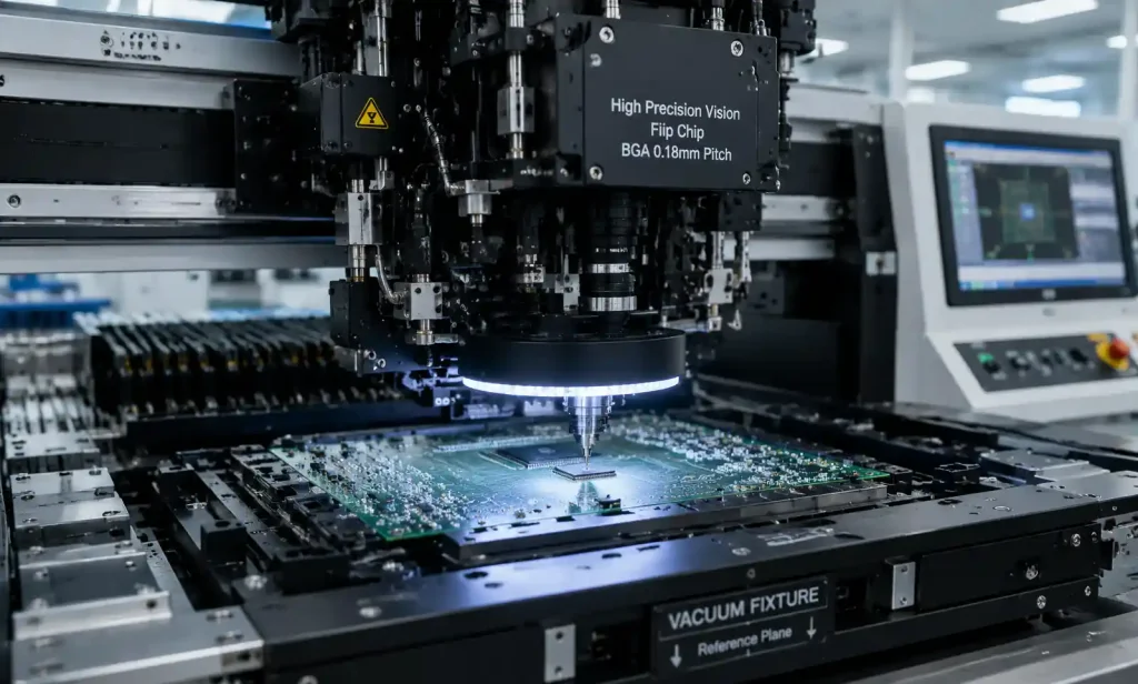
Pick-and-place equipment must provide placement accuracy of ±25 microns at 3-sigma, measured across the full work area. This typically requires high-end flip-chip capable placement systems with closed-loop vision correction and thermal compensation for machine drift. The placement head must have sufficient nozzle Z-axis control to accommodate small variations in component thickness without inducing tilt.
Vision system resolution becomes critical. The placement machine vision system must resolve features down to 5 microns to accurately locate both the component balls and PCB pads. Lighting must provide sufficient contrast to distinguish between the solder ball surface and the component body. Under-lighting or coaxial lighting configurations work better than standard ring lights for ultra-fine pitch components.
Solder paste printer requirements extend beyond standard specifications. The printer must provide ±15 micron print registration accuracy across the panel. Closed-loop vision alignment with fiducial recognition is mandatory. The print head pressure control must be programmable on a per-aperture basis to optimize paste release from the stencil apertures.
Stencil design parameters directly control paste volume delivery. For 0.18mm pitch BGAs, the stencil thickness typically ranges from 0.075mm to 0.100mm. Aperture size should provide 0.65-0.75 area ratio for optimal paste release. This means for a 0.10mm pad, the aperture opening would be 0.085-0.095mm with 0.075mm stencil thickness.
Conveyor systems and board handling must minimize mechanical stress. Boards with ultra-fine pitch BGAs are typically thinner (0.8-1.0mm) to accommodate microvia routing, making them more susceptible to handling-induced flexure. Center-support conveyor systems or vacuum hold-down fixtures help maintain board flatness during component placement.
5. Solder Paste and Reflow Profile Optimization
Solder paste selection and reflow profile development are the most process-sensitive aspects of 0.18mm pitch BGA assembly. The reduced thermal mass per joint and high joint density create a narrow process window that requires careful optimization.
Type 6 or Type 7 solder powder is required for 0.18mm pitch applications. Type 6 (25-45 micron particles) provides better printability and is suitable when stencil thickness is 0.100mm or greater. Type 7 (15-25 micron particles) becomes necessary when using thinner stencils or smaller apertures. Some assembly houses report better results with Type 7 for 0.18mm pitch despite the higher cost and shorter shelf life.
| Solder Paste Parameter | Type 6 Specification | Type 7 Specification | Selection Criteria |
|---|---|---|---|
| Powder size range | 25-45μm | 15-25μm | Aperture size vs. printability |
| Stencil thickness range | 0.100-0.125mm | 0.075-0.100mm | Print volume requirement |
| Typical aperture ratio | 0.70-0.80 | 0.65-0.75 | Release characteristics |
| Tack time @ 25°C | 4-6 hours | 2-4 hours | Production workflow |
| Working life after print | 6-8 hours | 4-6 hours | Line speed impact |
| Slump resistance | Excellent | Good | Bridge defect rate |
SAC305 (Sn96.5Ag3.0Cu0.5) remains the standard lead-free alloy for most applications, offering good joint reliability and reasonable reflow temperature. For applications requiring lower reflow temperature to reduce board warpage, SAC105 (Sn98.5Ag1.0Cu0.5) provides similar reliability with 5-7°C lower liquidus temperature.
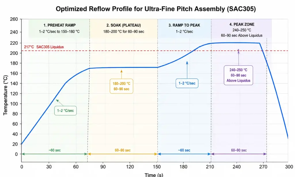
The reflow profile must be developed specifically for the combination of component package, board thickness, and thermal mass distribution. A typical profile for 0.18mm pitch BGA assembly uses a 4-zone reflow oven with the following guidelines: preheat to 150-180°C at 1-2°C/sec ramp rate, soak at 180-200°C for 60-90 seconds to activate flux and reduce thermal shock, ramp to peak at 1-2°C/sec, and achieve peak temperature of 240-250°C for SAC305 with time above liquidus of 60-90 seconds.
Component-specific limitations often constrain the profile more than solder requirements. Large BGAs with 0.18mm pitch frequently have maximum temperature ratings of 250°C or maximum time above 230°C ratings of 120 seconds. Profile development must verify that all locations within the BGA footprint, measured with thermocouples attached to representative pads, remain within component specifications while still achieving complete solder reflow.
Nitrogen atmosphere reflow can reduce voiding and improve wetting for 0.18mm pitch BGAs, particularly when using OSP or ImAg surface finishes. Maintaining oxygen levels below 100 ppm throughout the profile can reduce voiding by 30-50% and improve joint appearance, though the cost and complexity must be justified by yield improvement or reliability requirements.
6. X-ray Inspection and Quality Control Methods
At 0.18mm pitch, visual inspection and standard AOI cannot verify solder joint quality. X-ray inspection becomes the primary quality verification method, but not all X-ray systems provide adequate resolution or image quality for reliable defect detection.
The X-ray system must provide geometric magnification of at least 50x to adequately resolve 0.10mm solder balls. Detector resolution should be 10 microns or better at the magnification level used for inspection. Oblique angle X-ray capability (20-45 degree viewing angles) helps distinguish between bridging and closely-spaced joints that may appear connected in top-down view.
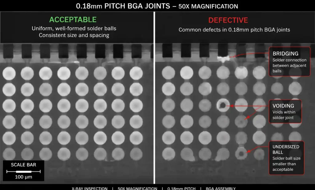
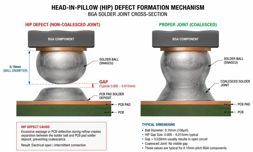
Key defects detectable by X-ray inspection include bridging between adjacent balls, where the solder has formed a continuous connection; insufficient solder volume, appearing as undersized or irregular ball shapes; voiding within the solder joint, particularly central voids exceeding 25% of ball area; and head-in-pillow defects, where the component ball and PCB solder deposit fail to coalesce.
X-ray inspection programming must account for the high ball count typical of 0.18mm pitch BGAs. Automated defect detection algorithms should be trained on known good and defective samples specific to the 0.18mm pitch. Manual inspection of every joint on a 500+ ball BGA is impractical for production volumes; automated inspection with manual review of flagged defects provides the best balance of thoroughness and throughput.
Acceptance criteria must be defined based on IPC-A-610 Class 3 standards adapted for ultra-fine pitch. Bridging is a rejection criterion for all joint pairs. Voiding exceeding 25% of the joint cross-section requires rejection or additional analysis. Head-in-pillow defects always require rework. Ball size variation exceeding ±20% from nominal may indicate process drift requiring investigation.
Electrical test provides complementary verification to X-ray inspection. Flying probe or bed-of-nails testing can detect opens and shorts that may not be visible in X-ray images, such as non-wetting defects where the joint appears intact radiographically but lacks electrical continuity. For high-reliability applications, combining X-ray inspection with electrical test provides the most complete quality verification.
7. Common Defects and Troubleshooting Strategies
Despite careful process control, several defect modes occur more frequently with 0.18mm pitch BGAs compared to standard pitch components. Understanding the root causes enables targeted corrective action.
Bridging defects most commonly result from excessive solder paste volume or poor paste release from the stencil. Check stencil aperture size and verify area ratio is within 0.65-0.75. Nano-coating or laser texturing of stencil apertures can improve release. If bridging occurs systematically in specific board regions, verify board flatness and placement force uniformity. Placement head tilt or excessive downward force can squeeze paste out from under the component.
Head-in-pillow defects occur when component warpage during reflow prevents the BGA balls from contacting the molten solder on the PCB pads. This defect is strongly correlated with peak temperature and time above liquidus. Reducing peak temperature by 5°C or reducing time above liquidus can reduce component warpage and eliminate HIP defects, though this must be balanced against achieving complete solder reflow. Using lower-CTE laminates reduces board warpage contribution to HIP formation.
Voiding can be reduced by optimizing the solder paste flux chemistry and reflow profile. Rapid temperature ramps during the preheat phase trap flux volatiles in the molten solder. Extending the soak time to 90-120 seconds and reducing the ramp rate to peak temperature to 1°C/sec typically reduces voiding. For applications requiring void-free joints, vacuum reflow or formic acid atmosphere reflow may be necessary.
Insufficient solder volume can result from via wicking, paste slumping before reflow, or inadequate stencil aperture size. If vias are present within the BGA footprint, verify they are completely filled and plated over. Check paste viscosity and ensure environmental conditions remain within specification during the time between printing and reflow. Increasing stencil thickness or aperture size can provide additional paste volume, but must be balanced against increased bridging risk.
Placement offset defects appear as systematic shifts in component position relative to the pad pattern. Verify pick-and-place machine calibration and vision system focus. Temperature gradients across the machine work area can cause thermal expansion that manifests as position drift. Some high-end placement systems compensate for thermal drift through closed-loop measurement and correction.
8. FAQ
What is the minimum PCB manufacturing capability required for 0.18mm pitch BGA assembly?
You need LDI solder mask capability with ±25 micron registration tolerance, ±50 micron layer-to-layer registration for HDI stackups, and board flatness controlled to 0.3% or better. Microvia capability (laser-drilled 0.10mm vias) is essential for routing escape unless the BGA has perimeter I/O only. Standard PCB shops without HDI capability cannot reliably support 0.18mm pitch designs.
Can I use the same reflow profile for 0.18mm pitch BGAs as I use for 0.4mm pitch components?
Generally no. The reduced thermal mass per joint and higher joint density require profile optimization specific to 0.18mm pitch. You typically need longer soak time (90+ seconds vs 60 seconds) and more controlled ramp rates to minimize warpage-induced defects. Profile development with thermocouple monitoring is essential rather than using generic profiles.
What X-ray magnification is needed to inspect 0.18mm pitch solder joints reliably?
Minimum 50x geometric magnification with 10 micron detector resolution. Lower magnification may show gross defects like missing balls but cannot reliably detect bridging or voiding. Oblique angle viewing (20-45 degrees) significantly improves defect detection versus top-down imaging alone.
Is nitrogen reflow necessary for 0.18mm pitch BGA assembly?
Not always necessary but beneficial. Air reflow can achieve acceptable results with ENIG surface finish and proper profile optimization. Nitrogen atmosphere (below 100 ppm O2) reduces voiding by 30-50% and improves wetting, especially with OSP or ImAg finishes. The cost is justified mainly for high-reliability applications or when yield improvement offsets the operating expense.
What are the typical yield rates for 0.18mm pitch BGA assembly in production?
First-pass yield typically ranges from 85-95% for established processes with appropriate equipment. Yields below 85% indicate process issues requiring optimization. Achieving 95%+ requires mature processes, optimal equipment, and tight material controls. Rework of 0.18mm pitch BGAs is challenging; most reworked boards require X-ray verification.
Can I rework 0.18mm pitch BGAs if defects are found?
Yes, but with significant constraints. You need a precision rework station with controlled hot air or IR heating, programmable temperature profiles, and placement accuracy comparable to production equipment. Rework success rate is typically 60-80% versus 95%+ for standard pitch components. Multiple rework attempts on the same site often cause pad lifting due to the small pad size.
What solder paste type gives the best results: Type 6 or Type 7?
Type 7 (15-25 micron powder) generally provides better results for 0.18mm pitch when using 0.075-0.100mm stencil thickness, though it costs 20-30% more and has shorter tack time. Type 6 (25-45 micron) can work adequately with 0.100mm stencils if print process is well-controlled. Run trials with both types on your specific design before committing to production.
How do I verify that my assembly equipment is capable of 0.18mm pitch before committing to a design?
Request a process capability study from your assembly house. They should demonstrate ±25 micron placement accuracy at 6-sigma, provide X-ray images showing their inspection capability, and show first-pass yield data from similar pitch assemblies. If they cannot provide this data or have no 0.18mm pitch production experience, consider that a significant risk.
9. Conclusion and Recommended Next Steps
Assembling 0.18mm‑pitch BGAs is a different beast compared to standard SMT. Everything—design, PCB fabrication, and assembly—has to work together with much tighter tolerances than 0.4mm parts.Design is where you win or lose. Use NSMD pads with proper solder mask openings, put copper‑filled vias under the BGA, and plan an HDI stackup for routing out. Pick low‑CTE laminates and keep the board flat—warpage kills joints during reflow.On the assembly side, focus on three things: Type 6 or 7 solder paste with a well‑tuned stencil, a pick‑and‑place machine that holds ±25 µm accuracy with vision feedback, and a reflow profile tailored to your specific board‑component combination. And X‑ray inspection isn’t optional—it’s the only way to see what’s going on under the ball.
Before you hit production, vet your assembly partner. Ask for placement data, X‑ray samples, and first‑pass yields from similar jobs. Run a process capability study specific to 0.18mm pitch—it’s the only way to be sure they’re ready.If you’re working with these fine‑pitch BGAs, talk to your PCB fab and assembly house before you start layout, not after. Early DFM conversations catch constraints that affect part choice, routing, and stackup.
Need a second pair of eyes? Our assembly team can do a free DFM review of your Gerbers and BOM. We’ll spot yield risks before you pay for tooling.