Heavy Copper PCB Assembly (6 OZ): Thermal Management Best Practices
Table of Contents
- What This Thermal Management Guide Covers
- Understanding 6 OZ Heavy Copper: Critical Thermal Properties
- Design Parameters for Optimal Heat Dissipation
- Thermal Management Strategies and Layer Stackup Design
- Manufacturing Considerations and DFM Guidelines
- Material Selection for High-Power Applications
- Frequently Asked Questions
- Conclusion and Next Steps
1. What This Thermal Management Guide Covers
Heavy copper PCB assemblies with 6 OZ copper weight have become essential for high-power applications where thermal dissipation is critical to system reliability. Unlike standard 1 OZ or 2 OZ boards, 6 OZ heavy copper PCBs can handle current loads exceeding 20 amperes per trace while simultaneously serving as integral heat spreaders within the assembly.
This guide addresses the unique thermal management challenges faced by power electronics engineers, PCB designers working on inverter systems, motor controllers, and high-power LED applications. You’ll learn how to leverage the thermal conductivity advantages of 6 OZ copper—approximately 200 times better than FR4—while navigating the manufacturing constraints that come with thicker copper layers.
Whether you’re designing an automotive ECU with demanding thermal cycling requirements, an industrial power supply operating at elevated ambient temperatures, or a renewable energy converter handling kilowatt-level power densities, this guide provides the design rules, material selection criteria, and DFM best practices you need to achieve reliable thermal performance.
We’ll cover trace width calculations for current carrying capacity, thermal via array design, copper balancing requirements specific to heavy copper boards, and how to work with PCB manufacturers to avoid common fabrication issues like uneven etching and excessive copper stress.
2. Understanding 6 OZ Heavy Copper: Critical Thermal Properties
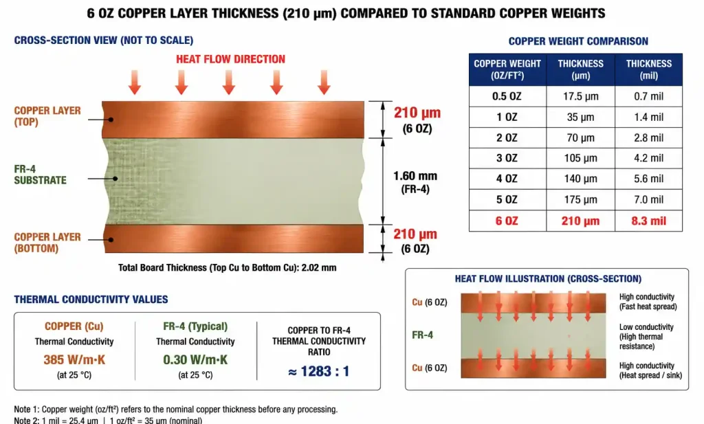
Heavy copper PCBs are defined by finished copper thickness greater than 3 OZ (105 μm). At 6 OZ, the finished copper thickness reaches approximately 210 μm (8.3 mils), which fundamentally changes both the electrical and thermal behavior of the circuit board.
The thermal conductivity of copper is approximately 385 W/(m·K), making it an exceptional heat conductor compared to standard FR4 substrate material at roughly 0.3 W/(m·K). This 1000:1 ratio means that in a 6 OZ heavy copper design, heat flows preferentially through the copper planes and traces rather than through the dielectric material.
From a current carrying perspective, 6 OZ copper can handle approximately 3 times the current density of 2 OZ copper for the same temperature rise. For a 100 mil (2.54 mm) wide trace in 6 OZ copper with a 10°C temperature rise allowance in free air, the current carrying capacity reaches approximately 15-18 amperes, compared to only 5-6 amperes for the same trace geometry in 1 OZ copper.
However, the thermal mass of 6 OZ copper also creates challenges during manufacturing. The thicker copper requires longer etching times, which can lead to undercutting and reduced trace width accuracy. The coefficient of thermal expansion (CTE) mismatch between heavy copper and FR4 substrate (17 ppm/°C for copper versus 14-17 ppm/°C for FR4 in the XY plane) becomes more pronounced, potentially causing stress-related failures during thermal cycling.
For thermal management design, the key advantage of 6 OZ copper is its ability to spread heat laterally across the board. A solid 6 OZ copper plane can reduce hot spot temperatures by 15-25°C compared to standard 1 OZ copper in high-power applications, effectively turning the entire copper layer into a heat spreader that complements external heatsinks and thermal interface materials.
3. Design Parameters for Optimal Heat Dissipation
Designing for thermal performance with 6 OZ heavy copper requires careful attention to trace geometry, copper distribution, and thermal via placement. The following parameters directly impact heat dissipation effectiveness.
Trace Width and Current Capacity
For 6 OZ copper, trace width must account for both electrical current requirements and thermal dissipation needs. The IPC-2221 standard provides the baseline calculation, but practical design should include additional margin for high-reliability applications.
| Trace Width (mils) | Current Capacity (A) at 10°C Rise | Current Capacity (A) at 30°C Rise | Voltage Drop per Inch (mV at max I) |
|---|---|---|---|
| 50 | 8.5 | 13.2 | 42 |
| 100 | 15.8 | 24.5 | 22 |
| 200 | 28.5 | 44.2 | 12 |
| 300 | 40.2 | 62.5 | 8 |
| 500 | 63.8 | 99.0 | 5 |
These values assume external copper layers in free air. For internal layers, reduce current capacity by approximately 40-50% due to reduced convective cooling. When traces carry sustained high current, widen them beyond the minimum electrical requirement to serve as additional heat spreading paths.
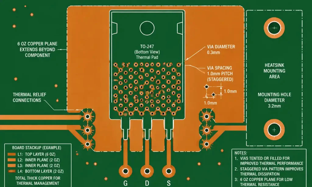
Thermal Via Arrays
Thermal vias transfer heat from component mounting areas through the board to copper planes or external heatsinks. For 6 OZ copper boards, thermal via design requires balancing via density against manufacturing capability.
Recommended thermal via specifications for heavy copper boards:
- Via diameter: 0.3-0.4 mm (12-16 mils) finished hole size
- Via pad diameter: 0.6-0.8 mm to accommodate 6 OZ copper pad fabrication tolerances
- Via spacing: minimum 0.6 mm (24 mils) center-to-center to maintain structural integrity
- Array pattern: staggered grid with 0.8-1.2 mm pitch for optimal thermal conductivity
For a typical power semiconductor package (TO-247, D2PAK), a thermal via array of 20-30 vias can reduce junction-to-board thermal resistance by 30-40% compared to copper plane spreading alone. Each 0.3 mm thermal via contributes approximately 0.15-0.2 W/°C of thermal conductance through a 1.6 mm board thickness.
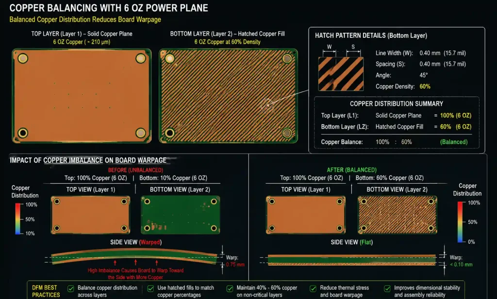
Copper Balance and Symmetry
Heavy copper boards are particularly susceptible to warping during fabrication and assembly due to unbalanced copper distribution. For 6 OZ copper layers, maintain copper balance within 30% between top and bottom layers, and within 40% between all layers in a multilayer stackup.
When one side requires dense 6 OZ copper planes for power distribution, add copper fill or hatched copper patterns to the opposite side. This balancing copper doesn’t need to be functional for electrical purposes—it serves primarily to maintain mechanical symmetry and prevent bow and twist during lamination and reflow.
4. Thermal Management Strategies and Layer Stackup Design
Effective thermal management in 6 OZ heavy copper assemblies requires strategic layer stackup design that optimizes heat flow paths from heat-generating components to heat dissipation structures.
Optimal Layer Stackup for Thermal Performance
For a 4-layer board with heavy copper requirements, the most thermally effective stackup places 6 OZ copper on external layers where components mount and convective cooling is most effective:
| Layer | Function | Copper Weight | Thickness (μm) | Notes |
|---|---|---|---|---|
| 1 (Top) | Component layer, power traces | 6 OZ | 210 | Direct component mounting and heatsink contact |
| 2 | Ground plane | 2 OZ | 70 | Thermal return path and EMI shielding |
| 3 | Power plane | 2 OZ | 70 | Power distribution and secondary heat spreading |
| 4 (Bottom) | Secondary component layer | 6 OZ | 210 | Balances top copper, provides thermal relief |
This asymmetric copper weight distribution concentrates heavy copper where thermal performance matters most while maintaining overall board balance. The 2 OZ internal planes provide electrical functionality without excessive board thickness or cost.
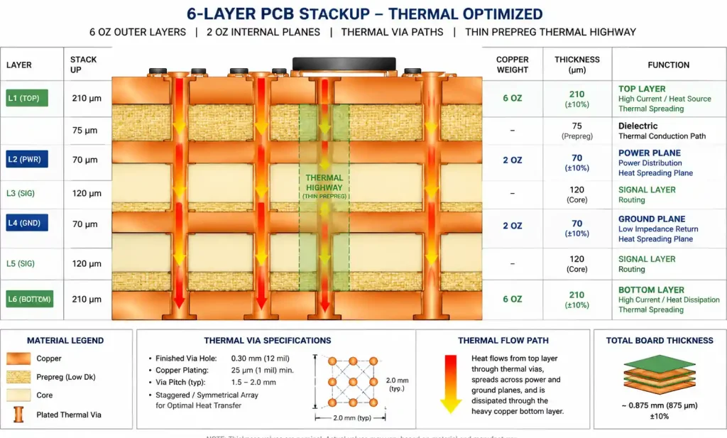
For 6-layer designs in high-power applications, consider a thermal core stackup that places two adjacent internal copper planes (2 OZ each) with thin prepreg separation (3-4 mils). This creates a high-conductivity thermal highway through the board center, effectively distributing heat from localized hot spots to larger copper areas.
Heat Spreading Techniques
Beyond basic copper weight, specific design techniques enhance thermal performance:
- Thermal relief modification: Standard thermal relief spokes for via connections impede heat flow. For thermal vias under power components, use solid connections or increase spoke width to at least 15 mils for 6 OZ copper.
- Copper flooding: Fill all unused board area with copper connected to ground or thermal planes. This maximizes the total copper mass available for heat absorption and spreading. Ensure copper flooding extends to within 20 mils of board edges to maximize thermal mass.
- Strategic trace routing: Route high-current traces to maximize copper area rather than minimum length. A 50 mil wider trace adds both current capacity and thermal dissipation area with minimal cost impact.
- Thermal plane segmentation: While solid planes provide maximum thermal conductivity, strategic segmentation can control heat flow direction. Use narrow copper bridges (50-100 mils wide) to thermally connect plane sections while maintaining electrical isolation for different power domains.
Component Placement for Thermal Optimization
Place heat-generating components near board edges or corners where external heatsinks can be mounted most effectively. Maintain minimum 10 mm spacing between high-power components (>2W dissipation each) to prevent thermal coupling where one component’s heat elevates another’s junction temperature.
For components requiring heatsinks, ensure the PCB copper beneath the component connects to solid 6 OZ copper planes extending at least 10 mm beyond the component footprint. This copper extension serves as a thermal pedestal that improves heat transfer to external heatsinks through thermal interface materials.
5. Manufacturing Considerations and DFM Guidelines
Heavy copper PCB fabrication introduces unique manufacturing challenges that directly impact thermal performance if not properly addressed during design.
Etching and Trace Definition
At 6 OZ copper thickness, the etching process requires significantly longer exposure to etchant chemicals compared to standard copper weights. This extended etching time causes increased undercutting—the lateral etching that occurs beneath the photoresist mask. For 6 OZ copper, expect approximately 6-8 mils of undercut per side, meaning a trace designed at 100 mils width may finish at 88-92 mils.
To compensate for this effect, designers should apply trace width compensation factors provided by the PCB manufacturer. Most manufacturers capable of 6 OZ copper processing can hold ±3 mils trace width tolerance, but this requires design rules that account for the undercut:
- Minimum trace width: 15 mils (design), 12 mils (finished)
- Minimum spacing: 15 mils for 6 OZ copper
- Trace width compensation: add 6-7 mils to designed width for critical dimensions
For thermal management traces where width directly affects current capacity and heat spreading, specify the required finished trace width on fabrication drawings and let the manufacturer apply appropriate compensation during CAM processing.
Plating and Hole Quality
Thermal vias in heavy copper boards require special attention during plating. The aspect ratio (board thickness divided by hole diameter) should not exceed 8:1 for reliable plating coverage. For a 2.0 mm thick board with 6 OZ copper, use minimum 0.25 mm (10 mil) drill diameter for through-hole vias.
The copper plating thickness in via barrels should reach at least 25 μm (1 mil) for IPC Class 2 requirements, but thermal applications benefit from heavier via plating—35-50 μm—to maximize thermal conductivity through the board thickness. Specify “filled and plated” or “plugged and plated” vias for thermal arrays to eliminate air gaps that impede heat transfer.
Lamination and CTE Management
The thermal mass of 6 OZ copper affects lamination press cycles, requiring longer heating and cooling times to ensure proper resin flow and avoid delamination. The CTE mismatch between heavy copper and substrate becomes critical during both fabrication and end-use thermal cycling.
DFM guidelines for heavy copper lamination:
- Avoid large solid copper areas exceeding 10 square inches without relief patterns
- Use copper crosshatching or grid patterns (50-80% copper fill) in large plane areas to reduce CTE stress
- Maintain balanced copper distribution across all layers to prevent laminate stress
- Specify high-Tg materials (minimum Tg 170°C) for applications with operating temperatures above 100°C
Solder Mask and Surface Finish Considerations
Heavy copper creates significant topography on the board surface—up to 8-10 mils of height difference between copper areas and substrate. This topography challenges solder mask application, potentially causing voids or thin spots that compromise insulation.
For 6 OZ copper boards:
- Specify increased solder mask thickness (2-3 mils build-up) to ensure adequate coverage over copper edges
- Use liquid photoimageable (LPI) solder mask rather than dry film for better edge coverage
- Avoid placing fine-pitch components (< 0.5 mm pitch) directly adjacent to heavy copper power planes
For thermal management, surface finish selection impacts heat transfer to external heatsinks. ENIG (Electroless Nickel Immersion Gold) provides a flat, reliable surface for thermal interface materials, while HASL (Hot Air Solder Leveling) creates an uneven surface that reduces thermal contact area. For components requiring optimal thermal coupling, specify ENIG on thermal pads and component mounting areas.
6. Material Selection for High-Power Applications
Substrate material selection significantly impacts thermal management performance in heavy copper PCBs, particularly for applications operating at elevated temperatures or requiring long-term reliability.
FR4 Variants and Thermal Performance
Standard FR4 with Tg 130-140°C is generally inadequate for heavy copper high-power designs due to thermal degradation risks above 120°C operating temperature. For power electronics applications, specify high-Tg FR4 variants or specialty materials:
| Material Type | Tg (°C) | Td (°C) | Thermal Conductivity (W/m·K) | CTE Z-axis (ppm/°C) | Application Suitability |
|---|---|---|---|---|---|
| Standard FR4 | 135 | 310 | 0.3 | 70 | Not recommended for 6 OZ heavy copper |
| High-Tg FR4 | 170 | 340 | 0.35 | 55 | Automotive, industrial control |
| FR4 + ceramic filler | 175 | 350 | 0.6-0.9 | 50 | High-power LED, motor drives |
| Polyimide | 250 | 390 | 0.4 | 40 | Aerospace, extreme environment |
| IMS (metal core) | 130 | N/A | 1.5-3.0 | 45 | High-power LED, power modules |
The thermal conductivity of standard FR4 creates a bottleneck for heat transfer through the board thickness. For applications where heat must transfer from components through the PCB to a heatsink on the opposite side, consider thermally enhanced materials with ceramic fillers that increase through-thickness thermal conductivity by 2-3x compared to standard FR4.
Specialized Thermal Materials
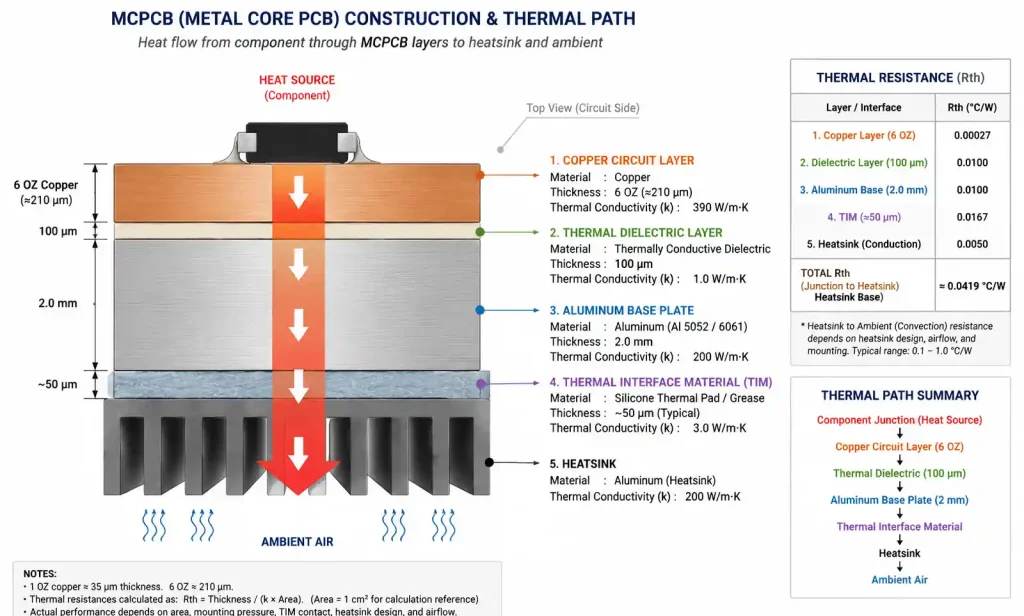
For extreme thermal management requirements, metal core PCBs (MCPCB) combine 6 OZ copper circuit layers with an aluminum or copper base plate separated by a thin dielectric layer. This construction provides thermal conductivity of 1.5-3.0 W/(m·K) through the dielectric while maintaining electrical isolation.
MCPCB designs are particularly effective for high-power LED arrays, power amplifiers, and motor controllers where the assembly mounts directly to a chassis or external heatsink. The metal core serves as both a structural element and a highly effective heat spreader, reducing thermal resistance from junction to ambient by 40-60% compared to FR4-based designs.
When specifying MCPCB with 6 OZ copper, consider:
- Dielectric thickness: 75-150 μm for optimal thermal performance
- Dielectric breakdown voltage: minimum 2.5-3.0 kV for high-voltage applications
- Metal core thickness: 1.5-3.0 mm aluminum for structural rigidity and thermal mass
- Surface insulation resistance: >100 MΩ to ensure electrical isolation
Material Selection Decision Framework
Choose substrate material based on these thermal and reliability criteria:
- Operating temperature: If component junction or ambient temperature exceeds 100°C continuous operation, specify minimum Tg 170°C material.
- Thermal cycling requirements: Automotive and industrial applications require materials with low CTE mismatch. Use high-Tg FR4 with controlled CTE (< 55 ppm/°C Z-axis) or polyimide for extreme cycling.
- Through-board thermal transfer needs: If heat must conduct through board thickness to a backside heatsink, specify thermally enhanced FR4 or MCPCB construction.
- Regulatory requirements: UL recognition (UL94 V-0 flammability rating) is standard for power electronics. Some applications require specific material certifications like automotive AEC-Q200 or aerospace IPC-6012 Class 3.
7. Frequently Asked Questions
What is the minimum trace width for 6 OZ copper PCB?
Most manufacturers capable of 6 OZ copper processing specify 15 mils minimum trace width and spacing. However, the finished trace width after etching undercut may be 12-13 mils. For critical thermal management traces, design with 20 mils minimum width to ensure adequate current carrying capacity and heat spreading after manufacturing tolerances.
How do I calculate thermal via array requirements for power components?
Start with the component’s thermal resistance requirement and board thermal resistance target. Each 0.3 mm diameter thermal via through a 1.6 mm board contributes approximately 0.15-0.2 W/°C thermal conductance. For example, to achieve 2 W/°C thermal conductance from component to bottom copper plane, you need approximately 10-13 thermal vias in the array beneath the component. Increase via count by 30-40% for designs requiring high reliability margins.
Can I mix 6 OZ copper with standard 1 OZ copper on the same PCB?
Yes, most advanced PCB manufacturers support mixed copper weights within a single board. Typically, specify 6 OZ on the layers requiring high current capacity and thermal dissipation (usually outer layers), and 1-2 OZ on internal signal layers. This approach optimizes thermal performance while controlling board thickness and cost. Ensure your manufacturer confirms they can maintain copper balance and lamination quality with mixed weights.
What spacing do I need between 6 OZ copper traces for high voltage applications?
Spacing requirements depend on voltage level and IPC class. For IPC-2221 Class 2, minimum spacing at 300V is 20 mils between conductors, increasing to 100 mils at 500V. However, for 6 OZ copper, the significant trace height (8+ mils) creates sharp edges that concentrate electric fields. Add 30-40% spacing margin beyond IPC minimums for high-voltage designs with heavy copper. For 500V applications, use 130-140 mils spacing rather than the 100 mil IPC minimum.
How does 6 OZ copper affect PCB lead time and cost?
Heavy copper processing typically adds 3-5 days to standard lead times due to extended etching, plating, and lamination cycles. Cost premium ranges from 30-60% compared to standard 1 OZ copper boards, depending on layer count and total board area. For prototype orders, expect higher premiums; volume production (>100 pieces) typically offers better pricing. Order sample boards early to validate thermal performance before committing to volume production.
Do I need special assembly considerations for 6 OZ heavy copper PCBs?
Yes, the increased thermal mass of 6 OZ copper requires adjusted reflow profiles. The board absorbs more heat during reflow, requiring 15-25% longer preheat and soak times to reach proper reflow temperature. Work with your assembly house to develop a validated thermal profile using test boards. For wave soldering, the higher thermal mass may require reduced conveyor speed or increased preheat zone temperature. Hand soldering requires higher wattage irons (80-100W) and longer dwell times compared to standard PCBs.
8. Conclusion and Next Steps
Heavy copper PCBs with 6 OZ copper are all about thermal muscle. They handle high currents and spread heat far better than standard copper—perfect for power electronics that run hot. But success depends on getting trace geometry, thermal vias, material choice, and manufacturing limits to play nicely together.For automotive power or motor controls, go big on copper area for spreading heat, but keep the distribution balanced to avoid warping. Use high‑Tg material (at least 170 °C) and talk early with your fab about design rules—heavy copper etches differently, so trace width, spacing, and vias need special attention.
Before you finalize, run thermal simulation that includes copper layout, via arrays, and component placement. Catching issues like insufficient via density, undersized traces, or unbalanced copper in design costs peanuts compared to fixing it after fabrication.If you’re pushing above 50 W or 10 A continuous, get your PCB manufacturer’s CAM team involved early. They’ll spot manufacturability hiccups and suggest tweaks that boost both thermal performance and yield.
Ready to move forward? Grab our heavy copper design checklist, or send us your Gerbers for a free DFM review focused on thermal optimization. We’ll look at copper distribution, via placement, and materials to make sure your design performs and builds reliably.