
Flexible PCB Design Challenges in Smart Wearable Devices: Engineering Guide for Smartwatches and VR Headsets (2026)
Smart wearable devices need PCBs that survive constant flexing, fit into tight curved spaces, and maintain electrical performance under mechanical stress. Smartwatches and VR headsets push flexible PCB design far beyond traditional rigid board rules. This guide covers the critical parameters—bend radius calculations, copper thickness trade-offs, material selection between polyimide and LCP, and DFM rules that actually matter for wearables.
Why Flexible PCBs Matter for Wearables
Wearables impose mechanical requirements that rigid PCBs can’t meet. Smartwatches need circuits that conform to curved wrists. VR headsets require lightweight boards that wrap around head geometry. Fitness trackers must survive millions of flex cycles. Flexible PCBs enable 3D packaging that reduces device thickness by 30-40% compared to rigid boards with connectors. For high-density wearables, rigid-flex eliminates board-to-board connectors entirely, improving reliability while cutting assembly costs.
Critical Design Parameters
Bend Radius and Copper Thickness
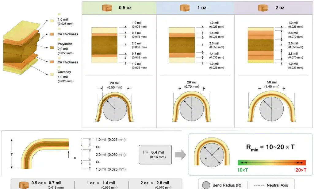
The relationship between copper weight and minimum bend radius is your most fundamental constraint. For dynamic flex applications—circuits that bend repeatedly during use—the minimum dynamic bend radius is typically 10-20 times the total material thickness. A two-layer flex with 1 oz copper and 2 mil polyimide requires about 3-4 mm minimum dynamic bend radius. Static flex (bent once during assembly) can use 6-10 times thickness.
Smartwatch designs constantly push these limits. The trade-off is copper thickness for current capacity versus flexibility for durability. Most wearables use 0.5 oz or 1 oz copper in dynamic flex sections, moving to thicker copper only in rigid areas. If you need 2 oz copper in a flex region for power, increase the bend radius proportionally—or accept copper cracking after 10,000-50,000 flex cycles.
Trace Routing Rules
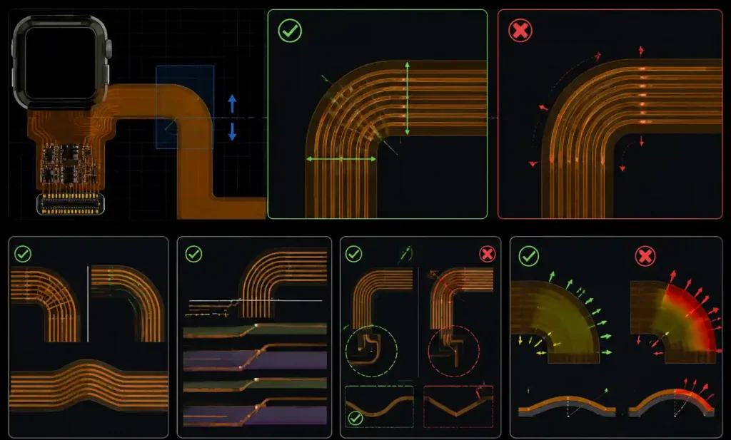
Trace orientation relative to the bend axis dramatically affects reliability. Route traces perpendicular to the bend line whenever possible, so they roll rather than stretch during flexing. When traces must run parallel to the bend, use curved traces instead of straight runs to distribute stress. Sharp 90-degree corners create stress concentration points that initiate cracking. All traces in flex sections should use curved or chamfered corners with minimum radii of 3-5 times trace width.
For multi-layer flex designs, stagger traces on different layers to avoid overlapping copper in the same location. This distributes stress more evenly and prevents delamination. For high-speed differential pairs in VR headsets, maintain consistent 50Ω or 100Ω impedance by adjusting trace width and spacing for polyimide’s dielectric constant (3.2-3.5) versus FR4’s 4.2-4.5.
Material Selection: Polyimide vs LCP
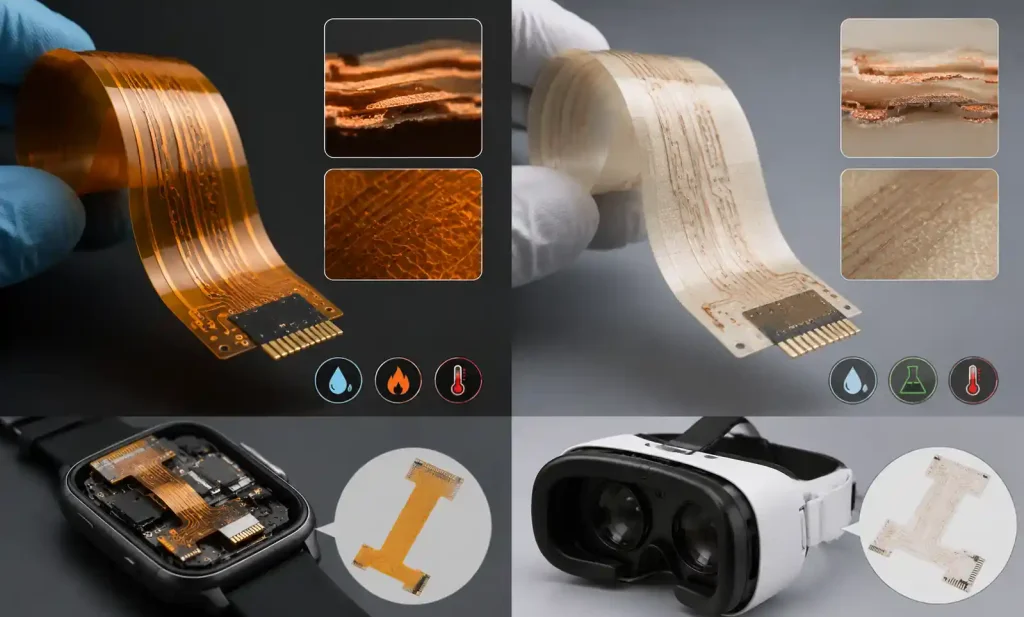
Polyimide is the default choice for smartwatches and fitness trackers. It handles 260°C reflow, offers decent dimensional stability, and works fine for most applications below 125°C continuous. Cost is predictable, and every flex manufacturer supports it.
Liquid crystal polymer (LCP) becomes the better choice for high-frequency wearables—VR headsets with 60 GHz WiGig or AR glasses with mmWave 5G. LCP offers lower dielectric loss (Df of 0.002-0.004 versus polyimide’s 0.01-0.02 at 10 GHz) and better dimensional stability across temperature. But LCP costs 2-3 times more and requires specialized processing that limits your manufacturer options. For most smartwatch designs running signals below 1 GHz, polyimide is the smarter choice.
Coverlay and Stiffener Selection
Standard 1 mil polyimide coverlay with 1 mil acrylic adhesive provides adequate protection while maintaining flexibility. In areas needing extra durability, consider 2 mil or 3 mil coverlay—but remember that thicker coverlay increases your minimum bend radius.
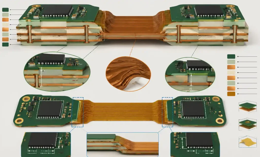
Stiffener placement is critical in rigid-flex designs. FR4 or polyimide stiffeners create localized rigid areas for component mounting while keeping interconnect regions flexible. For BGA components on smartwatch flex circuits, you typically need 0.4-0.8 mm stiffeners to prevent warpage during reflow. Position stiffeners at least 2-3 mm away from bend lines to avoid creating stress concentration zones.
Design Rule Comparison
| Design Parameter | Rigid PCB | Flexible PCB (Dynamic) | Rigid-Flex (Wearable) |
|---|---|---|---|
| Min trace width | 4 mils | 4-6 mils | 4 mils rigid / 6 mils flex |
| Min trace spacing | 4 mils | 6-8 mils | 4 mils rigid / 8 mils flex |
| Copper weight | 1-2 oz | 0.5-1 oz | 1 oz rigid / 0.5 oz flex |
| Min drill size | 8 mils | 10-12 mils | 8 mils rigid / 12 mils flex |
| Min annular ring | 2 mils | 4 mils | 2 mils rigid / 4 mils flex |
| Via aspect ratio | 10:1 | 6:1 | 8:1 rigid / 6:1 flex |
| Bend radius (dynamic) | N/A | 10-20× thickness | 12-15× thickness |
The wider spacing requirements in flex regions come from mechanical stress during bending—adjacent traces can short if spaced too closely. The reduced copper weight in dynamic flex zones trades current capacity for durability. You’ll need separate design rule sets for rigid and flex regions in your EDA tool.
Note that annular ring doubles in flex sections. This provides margin against registration tolerances during drilling and accounts for material movement during flexing.
Layer Stackup Strategies
Most smartwatch applications use 2-layer or 4-layer flex constructions. A standard 4-layer flex stackup: signal-ground-ground-signal with 2 mil polyimide between layers and 0.5 oz copper. This symmetric stackup prevents curling and provides two ground planes for return current and shielding.
For VR headsets with higher density, 6-layer or 8-layer rigid-flex becomes necessary for high-speed video, power distribution, and sensor interfaces. Place high-speed differential pairs on outer layers for better impedance control and easier probing. Reserve inner layers for power and low-speed signals. Flex sections should use the minimum layers possible—typically 2—with layer transitions in rigid areas.
Impedance Control in Flex
Calculating trace impedance in flex requires adjusting for polyimide’s lower Dk. For a 50Ω single-ended trace on 2-layer flex with 2 mil polyimide and 0.5 oz copper, trace width is typically 6-8 mils, versus 5-6 mils on FR4 with 4 mil dielectric. The exact width depends on your manufacturer’s process tolerances and the specific polyimide Dk (3.2-3.5).
For differential pairs carrying high-speed USB, MIPI, or DisplayPort in VR headsets, target 100Ω differential impedance with 5-mil pair-to-pair coupling. Always request impedance test coupons on your panel and specify TDR test method with ±10% tolerance (typical for flex versus ±5% for rigid).
Material Property Comparison
| Material Property | Standard Polyimide | High-Tg Polyimide | LCP |
|---|---|---|---|
| Dk (1 GHz) | 3.4-3.5 | 3.2-3.3 | 2.9-3.0 |
| Loss tangent (10 GHz) | 0.01-0.02 | 0.008-0.015 | 0.002-0.004 |
| Tg | 360°C | 410°C | None (crystalline) |
| Moisture absorption | 1.8-2.5% | 1.2-1.8% | 0.04% |
| CTE | 20-40 ppm/°C | 16-25 ppm/°C | 12-17 ppm/°C |
| Cost multiplier | 1× | 1.3-1.5× | 2.5-3× |
| Best for | Smartwatches, trackers | Medical, automotive | VR/AR, mmWave |
Polyimide remains the dominant choice for consumer wearables despite LCP’s superior electrical properties. For a typical smartwatch operating below 2.4 GHz, polyimide provides adequate performance at baseline cost. LCP’s low moisture absorption (0.04%) prevents dimensional changes and maintains stable electrical properties in wet conditions—valuable for VR/AR with 60 GHz links, but overkill for most smartwatches.
DFM Considerations and Common Pitfalls
Flex-to-Rigid Transitions
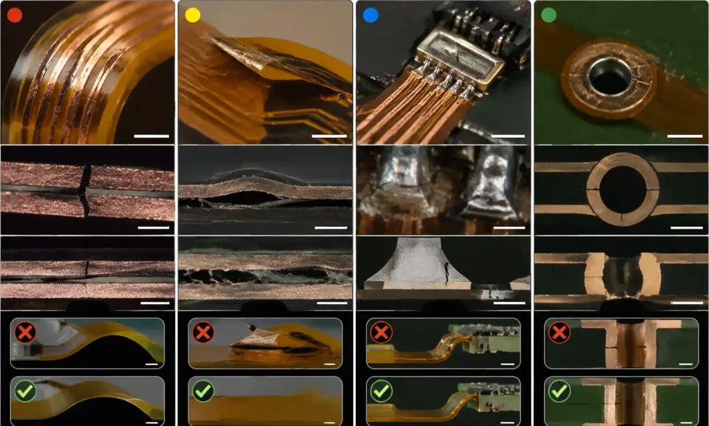
The junction between rigid and flexible sections is the highest stress point and the most common failure location. Create gradual transitions by extending the flex material 1-2 mm beyond the stiffener edge. Avoid vias or components within 3 mm of the transition zone—differential expansion during thermal cycling cracks solder joints or via barrels.
In smartwatch designs where the board wraps around the device perimeter, map out your bend profiles in 3D CAD before starting PCB layout. Coordinate with mechanical engineering to ensure PCB bend geometry matches the enclosure with appropriate assembly tolerances.
Teardrops and Strain Relief
Teardrops are mandatory at all pad-to-trace junctions in flex circuits. They distribute mechanical stress and prevent trace lifting during flexing. Most EDA tools can generate them automatically. Verify that teardrop length is at least 2-3 times pad diameter and blends smoothly into the trace width without creating impedance discontinuities.
Panelization for Flex
Flex PCB panelization differs from rigid boards—you can’t route tabs and V-grooves through flex material without damaging it. Most manufacturers use perforated tabs or leave-in tabs removed manually after assembly. For rigid-flex, router depaneling works in rigid areas, but flex tails must extend beyond the routed edge. Specify depaneling method and tab locations on your fabrication drawing.
Reliability Testing for Wearables
Qualification testing must simulate the actual mechanical stress profile. Standard IPC-TM-650 mandrel bend tests don’t accurately represent complex 3D bending in smartwatches or VR headsets. Work with your manufacturer to develop application-specific test protocols replicating your device’s bend locations, angles, and cycle counts.
For dynamic flex applications (smartwatch bands, VR straps), target 100,000-200,000 flex cycles at design bend radius without failure. For static flex (assembly-only bending), 10 cycles without damage is typically sufficient. Accelerated thermal cycling from -40°C to 125°C reveals rigid-to-flex transition failures and coverlay delamination before field use.
Request cross-section analysis on first article PCBs to verify layer registration, copper thickness uniformity, and adhesion quality between polyimide and copper layers.
Common Design Errors
Based on CAM engineering experience, these are the most frequent mistakes:
Insufficient bend radius calculation — Calculate based on full material buildup in the bend area, not just flex material thickness alone.
Traces running parallel to bend lines — The single most common cause of copper cracking. Route perpendicular wherever possible.
Components too close to flex-to-rigid transitions — Thermal expansion mismatch creates high stress zones. Maintain at least 3 mm clearance.
Inadequate stiffener support for BGAs — 0.4-0.8 mm FR4 stiffeners are minimum for packages with pitch below 0.5 mm.
Mismatched impedance at layer transitions — Model transitions in your stackup tool and adjust trace widths accordingly.
FAQ
What is the minimum bend radius for a 4-layer flex PCB in a smartwatch?
For dynamic flex, calculate 12-15 times total thickness of your 4-layer stackup including coverlay. A typical 4-layer flex with 0.5 oz copper is approximately 0.25-0.3 mm thick, requiring 3-4.5 mm minimum dynamic bend radius. For static flex (assembly-only), you can reduce to 6-8 times thickness, or 1.5-2.5 mm.
Can I use standard FR4 rigid-flex boards for wearables, or must I use polyimide throughout?
Rigid-flex with FR4 rigid sections and polyimide flex sections is the most common construction for wearables. This hybrid gives you cost-effective rigid areas for component mounting and flexible interconnects for mechanical compliance. Pure polyimide throughout would be more expensive without significant benefits in typical smartwatch applications.
How do I calculate trace width for 50-ohm impedance on a 2-layer polyimide flex circuit?
Use your stackup calculator with: 2 mil polyimide dielectric (Dk = 3.4-3.5), 0.5 oz copper thickness, and ground plane on the opposite layer. Typical result is 6-8 mils trace width for 50 ohms. Verify with impedance test coupons on first article—polyimide Dk varies by manufacturer and grade.
What surface finish works best for flex circuits in wearable devices?
ENIG (Electroless Nickel Immersion Gold) is the standard choice because it provides excellent solderability, wire bonding compatibility, and oxidation resistance without high-temperature processing. Avoid HASL on flex circuits—the high temperature and mechanical stress during hot air leveling can damage thin polyimide substrates.
How many flex cycles should I design for in a smartwatch band application?
Target 100,000 to 200,000 flex cycles as minimum qualification for dynamic flex in smartwatch bands or VR headset straps. This represents roughly 1-2 years of daily use. Medical or industrial wearables may require 500,000+ cycles depending on duty cycle.
What copper weight should I use in flex sections of a rigid-flex board?
Use 0.5 oz copper in dynamic flex regions with repeated bending. Use 1 oz copper in static flex regions that bend only during assembly. Use 1-2 oz copper in rigid sections where you need higher current capacity. Never use 2 oz or thicker in dynamic flex areas unless you can accommodate significantly larger bend radii.
Conclusion
If your wearable flexes repeatedly during use (smartwatch bands, VR straps), prioritize bend radius and copper thickness as your first constraints. Use 0.5 oz copper, route traces perpendicular to bend axes, and target 12-15× material thickness for minimum bend radius. For static flex (assembly-only), you can relax to 6-8× thickness and consider 1 oz copper for better current capacity.
For high-frequency wearables with multi-gigabit video links or mmWave wireless, evaluate whether polyimide meets your signal integrity budget or if LCP’s lower loss justifies the 2-3× cost premium. For most smartwatch applications below 2.4 GHz, polyimide is the smarter choice.
Before submitting Gerbers, verify your EDA design rules enforce different clearances and annular rings for rigid versus flex regions. Run DRC with manufacturer-specific capabilities. Request a DFM review focusing on bend radius verification, layer transitions, and depaneling strategy.