
Understanding HDI Flex PCB: Advantages and Challenges of 3+N+3 Structure (2026)
The 3+N+3 HDI flex structure packs high-density routing into a bendable board—three HDI buildup layers on each side of a flexible polyimide core. It’s how foldable phones route signals across hinges and medical wearables fit complex circuits into tiny spaces. But this layered construction comes with manufacturing trade-offs: tighter registration tolerances, higher costs, and real risks if you put vias in the wrong place. Here’s what actually matters when designing one.
What Is 3+N+3 HDI Flex?
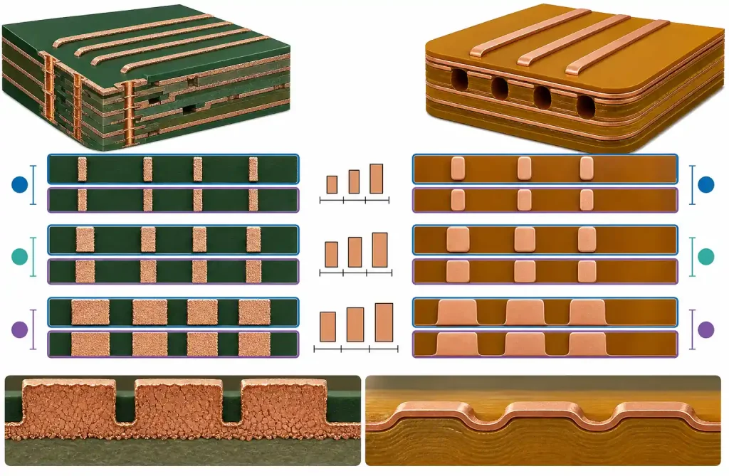
The “3+N+3” notation means three sequential lamination cycles on the top, then three on the bottom, wrapped around a flexible core (“N” layers of polyimide flex in the middle). The outer HDI layers use FR-4 or modified epoxy with electrodeposited copper for fine-line routing (50µm traces, laser-drilled microvias). The core uses polyimide with rolled-annealed copper—it bends, while the rigid sections handle dense BGA fanouts.
This hybrid construction replaces both a rigid PCB and a flex cable, eliminating connectors and saving space in foldable devices, medical implants, and aerospace instrumentation.
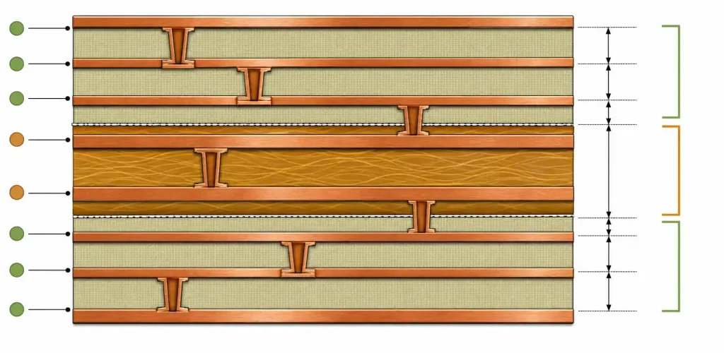
Key Advantages
Routing density on flex: With 0.1mm microvias and 0.2mm capture pads, you can fan out 0.4mm-pitch BGAs directly on the flex substrate without a separate rigid interposer. For foldable hinge boards carrying processor and memory die, this is non-negotiable.
No connectors, fewer failures: ZIF connectors and soldered FFC joints are failure points—contact resistance, mechanical wear, assembly yield loss. 3+N+3 eliminates them entirely. Automotive camera modules and robotic arms benefit from this reliability boost.
Controlled impedance across the boundary: Impedance changes as signals cross from FR-4 (Dk ~4.2–4.6) to polyimide (Dk ~3.4–3.6). But because both sections use similar copper and dielectric thicknesses, the discontinuity is manageable. Adjust trace width in the flex region to keep 50Ω or 100Ω differential impedance within ±10%—doable with proper stackup simulation.
Manufacturing Challenges
Sequential lamination: Six separate buildup cycles beyond the core flex (three top, three bottom). Each adds registration risk. Polyimide flex cores shift due to moisture and thermal expansion. Total misregistration budget can hit ±100 microns (4 mil) or more. Design rule: use 75-micron annular rings on microvias, not the 50-micron minimum IPC-6012 Class 2 might suggest.
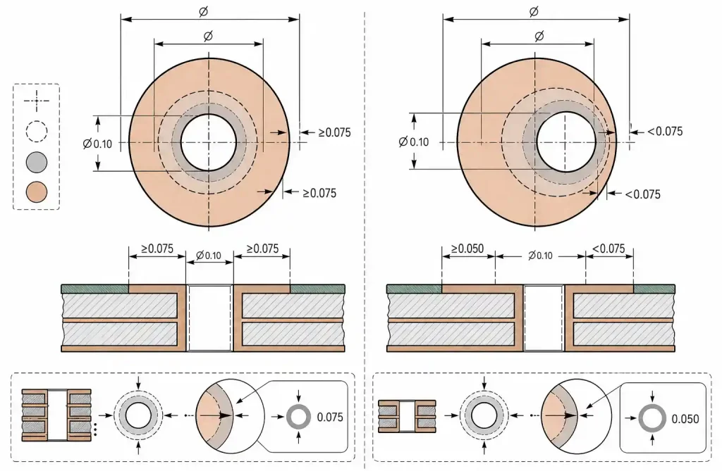
Core material limitations: Flex core uses rolled-annealed copper—softer, more ductile, essential for bending. But RA copper has a rougher surface, limiting minimum trace width. Most fabs reliably hold 75-micron (3 mil) trace/space on polyimide with RA copper; pushing to 50 microns (2 mil) kills yield.
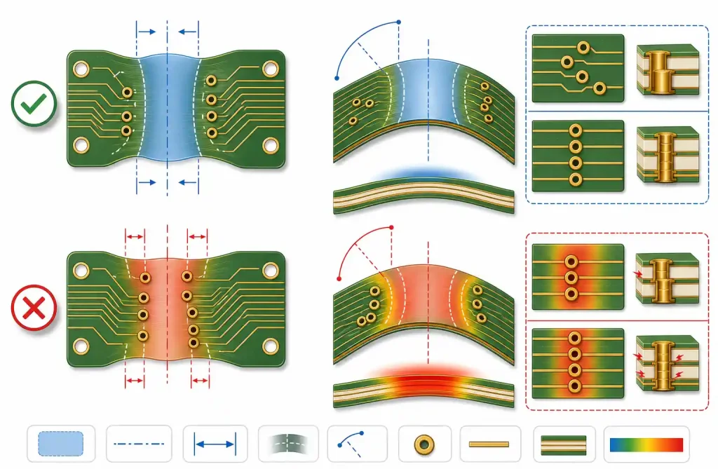
Microvias in flex zones: Copper-plated via barrels crack after thousands of flex cycles. Keep vias at least 3mm from the bend line. If you can’t, use staggered vias (not stacked) and consider a stiffener on the back side to reduce localized strain.
Design Rule Comparison by Application
| Parameter | Consumer (Class 2) | Medical/Automotive (Class 3) | Aerospace/Military (Class 3+) |
|---|---|---|---|
| Min trace/space (rigid HDI) | 50µm / 50µm (2/2 mil) | 75µm / 75µm (3/3 mil) | 100µm / 100µm (4/4 mil) |
| Min trace/space (flex core) | 75µm / 75µm (3/3 mil) | 100µm / 100µm (4/4 mil) | 125µm / 125µm (5/5 mil) |
| Microvia diameter (laser) | 0.1mm (4 mil) | 0.15mm (6 mil) | 0.2mm (8 mil) |
| Microvia capture pad | 0.2mm (8 mil) | 0.25mm (10 mil) | 0.3mm (12 mil) |
| Min annular ring | 50µm (2 mil) | 75µm (3 mil) | 100µm (4 mil) |
| Flex core copper | 18µm (0.5 oz) | 18µm (0.5 oz) | 35µm (1 oz) |
| Min bend radius (dynamic) | 10× thickness | 15× thickness | 20× thickness |
| IPC class | IPC-6013 Class 2 | IPC-6013 Class 3 | IPC-6013 Class 3 + MIL |
Consumer designs push density and lower cost. Medical and automotive need higher reliability margins—wider traces, larger annular rings. Aerospace adds another layer of process controls and qualification.
Material Selection & Stackup
Flex core: polyimide (Kapton, Apical) with Dk 3.4–3.6 at 1GHz. Rigid HDI layers: FR-4 for cost-sensitive designs; low-loss materials (Megtron 6, Isola I-Speed) for high-speed.
Typical 8-layer stack: three HDI layers top (L1-L3), two-layer flex core (L4-L5), three HDI layers bottom (L6-L8). Route controlled-impedance signals on L2 or L7—adjacent to ground planes. Put power/ground on L3, L4, L5, L6 for return paths and shielding.
Flex thickness rule: Keep the flex region under 0.3mm if you need bend radii below 3mm. Thicker flex won’t fold cleanly and cracks under repeated cycling. Standard polyimide Tg is ~250°C—fine for most applications, but some low-cost flex materials have lower Tg and won’t survive automotive under-hood temperatures.
Common DFM Errors
Vias in flex zones: Stacked microvias in the bend region is the #1 error. Copper in the via barrel isn’t as ductile as the surrounding foil, so bending concentrates stress and cracks the via. Keep vias ≥3mm from the bend line, or use staggered vias with a stiffener.
Insufficient copper-to-edge clearance: Traces perpendicular to the bend axis experience tensile stress on the outer surface. If they’re too close to the flex edge, you get delamination or copper cracking. Maintain ≥0.5mm clearance from any copper feature to the flex edge.
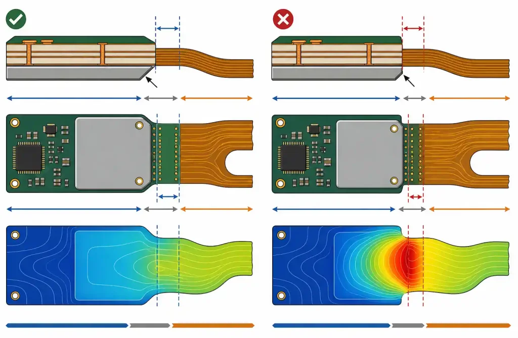
Stiffener design: Bonding a stiffener too close to the flex region creates a hard transition point that concentrates bending stress. Leave ≥1mm gap between stiffener edge and the dynamic flex zone. Use chamfered or tapered stiffener edges.
When to Use 3+N+3 vs Simpler Alternatives
Choose 3+N+3 when:
- BGA pitch ≤0.5mm on flex substrate
- Board folds repeatedly (>1,000 cycles) with high-speed signals
- Controlled impedance across rigid-flex boundary is required
- Weight/volume are critical (aerospace, wearables, implants)
- Eliminating connectors improves reliability or assembly
Consider simpler when:
- Standard flex (2–4 layers) with larger trace/space meets routing needs
- Static flex only (fold once during assembly) → rigid-flex with mechanical bend is simpler
- Routing density only needed in rigid sections → rigid HDI + FFC cable
- Cost is the primary constraint and design fits in 4–6 layers → standard rigid-flex
FAQ
What is the typical cost premium for 3+N+3 HDI flex versus standard rigid-flex?
Expect 2–3× cost increase over a standard 4–6 layer rigid-flex. Prototype runs (10–50 pieces) often hit 3–5×; volume production (1,000+ pieces) approaches 2× as yields improve.
Can I use ENIG on the flex core section?
Yes, ENIG works on polyimide flex cores and provides good solderability and wire bonding. But the nickel layer (3–5µm) adds stiffness, reducing flex cycle life. For maximum flexibility, consider immersion silver or OSP.
How do I calculate minimum bend radius for a 3+N+3 HDI flex design?
Static bending (one-time installation): 6× total thickness. Occasional flexing (<100 cycles): 10× total thickness. Dynamic flexing (>10,000 cycles): 20× total thickness or more. Measure thickness at the flex region only, excluding stiffeners.
What’s the difference between IPC-6013 Class 2 and Class 3 for HDI flex?
Class 3 requires larger annular rings (75µm vs 50µm), tighter impedance control (±10% vs ±15%), and stricter inspection criteria—including microsectioning for via quality verification. Class 3 is required for medical devices, automotive safety systems, and aerospace.
How should I route differential pairs across rigid-to-flex transitions?
Maintain constant trace spacing and coupling throughout. Use the same reference plane on both sides. If dielectric constant changes between rigid and flex sections, adjust trace width in the flex region to maintain target impedance—but keep spacing constant to preserve coupling. Simulate with a 2D field solver to verify impedance variation stays within ±10%.
What are the most common field failure modes for flex PCBs?
Copper fatigue from repeated bending (especially at via locations), delamination at rigid-flex interfaces, cracked solder joints on components too close to flex zones, and edge delamination from insufficient copper-to-edge clearance. Proper DFM review and bend testing during prototyping catch most of these.
Conclusion
3+N+3 HDI flex gives you high routing density in a bendable form factor—great for foldable devices, medical implants, and any space-constrained product where connectors are a liability. But the complexity is real: sequential lamination, registration tolerances, and flex zone via placement all demand careful design.
Before you commit: verify via placement relative to bend zones, confirm trace width/spacing meets manufacturer capabilities in both rigid and flex regions, check stiffener clearances, and validate impedance across transitions. Most leading fabs offer free DFM review for HDI flex designs—use it.
If your application needs high-density BGA fanout on a flex substrate or repeated bending with controlled impedance, 3+N+3 is worth the cost. For simpler needs, standard flex or rigid-flex will save you money and headaches.