
Rigid Flex PCB Design Guidelines: Avoid Common Mistakes
Rigid flex PCB design failures account for 30-40% of prototype rejections in electronics manufacturing. Improper bend radius calculations, incorrect copper weight selection, and poor via placement cause the majority of reliability issues and production delays in rigid flex circuits.
If you want to design reliable rigid flex PCB for wearable devices, medical equipment, or aerospace applications, you need to understand critical design rules, material selection, bend radius requirements, and manufacturing constraints that differ significantly from standard rigid PCB design.
What Makes Rigid Flex PCB Design Different?
Rigid flex PCB combines rigid FR4 sections with flexible polyimide layers in a single integrated assembly. This hybrid construction requires specialized design rules that account for mechanical stress, material properties, and manufacturing processes fundamentally different from traditional rigid PCB.
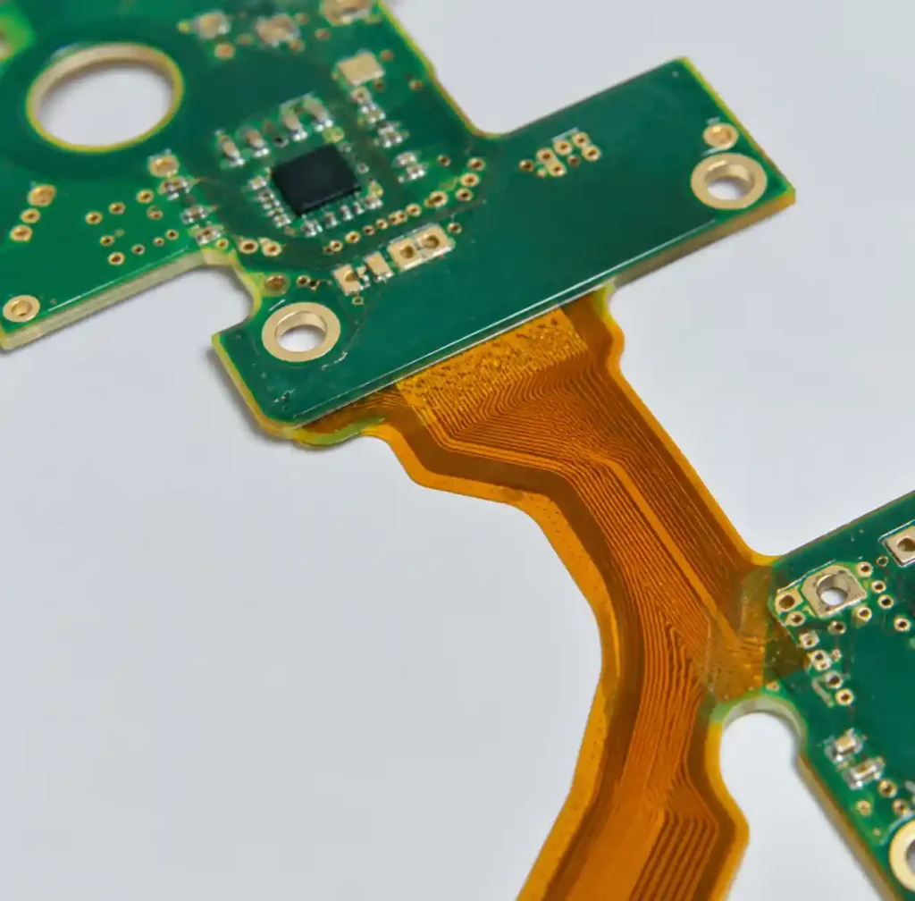
The flexible sections must withstand bending without copper cracking, delamination, or electrical failures. Rigid flex prototypes have 2-3× higher rejection rates than standard rigid boards due to design rule violations. Understanding these critical differences prevents failures and ensures first-time manufacturing success.
Mistake #1: Incorrect Bend Radius Calculation
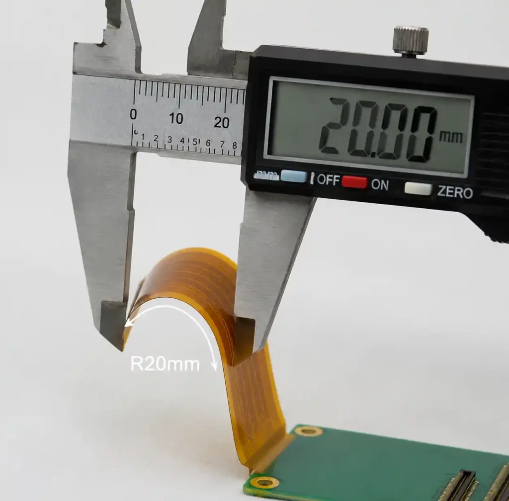
Minimum bend radius equals 10× total flex section thickness for dynamic flexing applications. For static bends (one-time installation), 6× thickness is acceptable.
| Flex Thickness | Static Bend Radius | Dynamic Bend Radius |
|---|---|---|
| 0.1mm (2-layer) | 0.6mm minimum | 1.0mm minimum |
| 0.2mm (4-layer) | 1.2mm minimum | 2.0mm minimum |
| 0.3mm (6-layer) | 1.8mm minimum | 3.0mm minimum |
| 0.4mm (8-layer) | 2.4mm minimum | 4.0mm minimum |
How to avoid: Calculate total flex section thickness including substrate, copper, adhesive, and coverlay. Add 20% safety margin. For dynamic applications requiring 100,000+ flex cycles, use 12-15× thickness for extended reliability.
Mistake #2: Wrong Copper Weight in Flex Sections
Heavy copper in flex sections creates stress concentration points and reduces flexibility. Use 0.5oz (½oz, 17μm) or 1oz (35μm) rolled-annealed copper in flex sections. Rolled-annealed copper has directional grain structure that withstands repeated bending better than electrodeposited copper.
| Copper Type | Thickness | Application | Flex Cycles |
|---|---|---|---|
| ½oz Rolled-Annealed | 17μm (0.7mil) | Dynamic flex, tight bends | 1,000,000+ |
| 1oz Rolled-Annealed | 35μm (1.4mil) | Static flex, moderate bends | 100,000+ |
| 2oz Electrodeposited | 70μm (2.8mil) | Rigid sections only | Not for flexing |
Design recommendation: Specify ½oz rolled-annealed copper for dynamic flex applications. Use 1oz for static flex. Reserve heavy copper (2oz+) for rigid sections. Work with your PCB manufacturer to verify specifications in fabrication drawings.
Mistake #3: Poor Via Placement in Flex Zones
Vias create rigid points that concentrate stress. Never place vias within the bend radius area or within 1mm (40mil) of the rigid-flex transition zone.
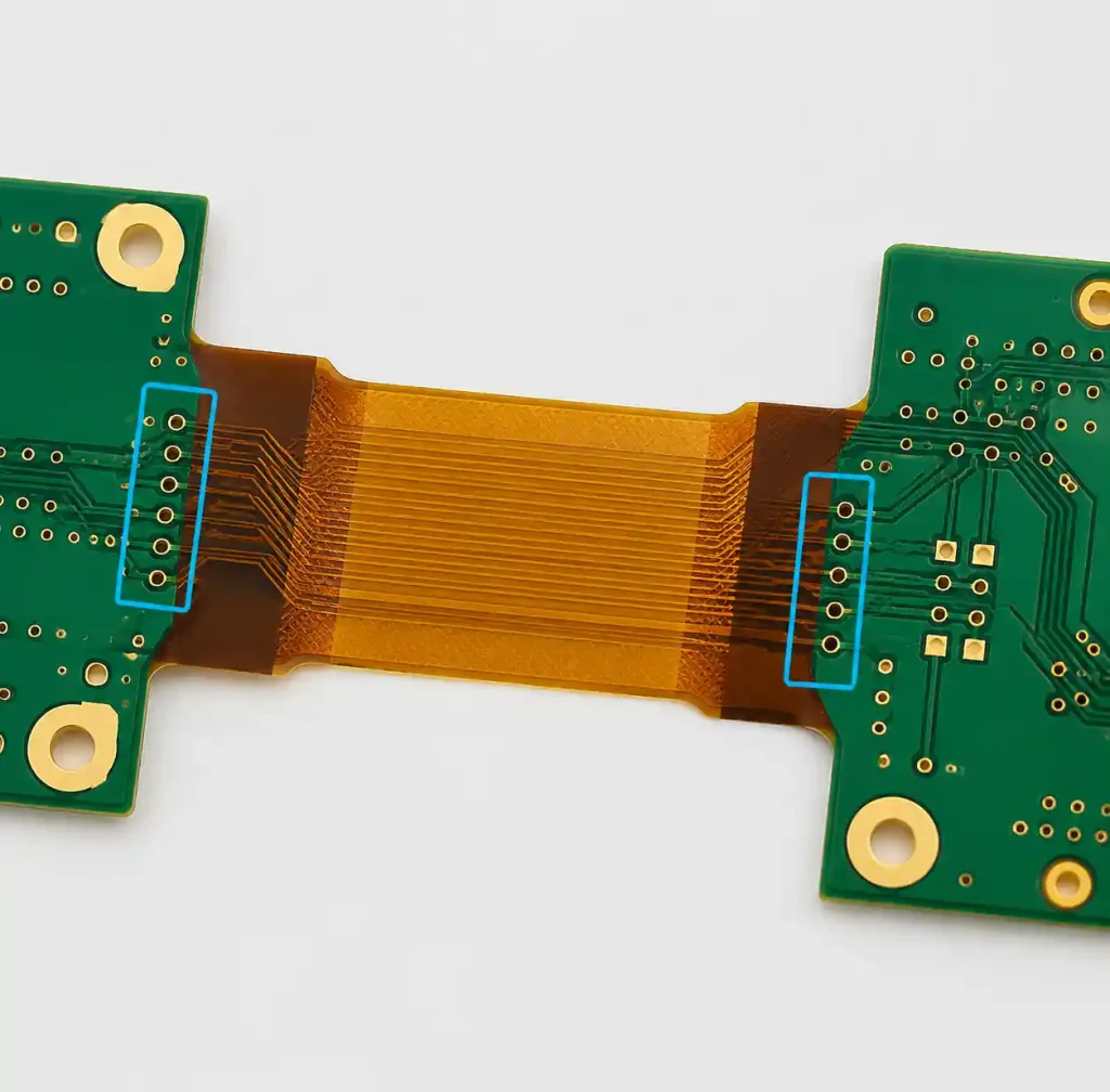
Via placement guidelines:
- Place all vias in rigid sections whenever possible
- If vias are unavoidable, locate them at the neutral bend axis
- Use filled vias in flex sections to prevent stress concentration
- Stagger via placement to avoid creating rigid lines
- Maintain minimum 0.5mm distance between vias in flex areas
Mistake #4: Improper Trace Routing Through Bends
Traces perpendicular to the bend axis experience maximum tensile stress. Route traces perpendicular to the bend axis (90° to bend direction). Use curved traces instead of sharp 90° angles. Maintain consistent trace width through flex sections. Use hatched copper pours instead of solid copper planes.
| Trace Configuration | Flex Reliability | Recommended Use |
|---|---|---|
| Perpendicular to bend (90°) | Excellent | All flex applications |
| Diagonal (45°) | Good | When perpendicular impossible |
| Parallel to bend (0°) | Poor | Avoid in flex zones |
| Solid copper pour | Very Poor | Never in flex sections |
Mistake #5: Neglecting Stiffener Design
Stiffeners provide mechanical support for connectors and components. Incorrect placement or improper attachment causes problems.
Proper stiffener design:
- FR4 stiffener (standard), polyimide (heat-resistant), or stainless steel (high strength)
- Stop stiffeners 1-2mm before bend radius begins
- Use tapered or beveled edges (not sharp corners)
- Specify proper adhesive (acrylic or PSA rated for operating temperature)
- Cover all connector and component mounting areas
Mistake #6: Inadequate Layer Stackup Planning
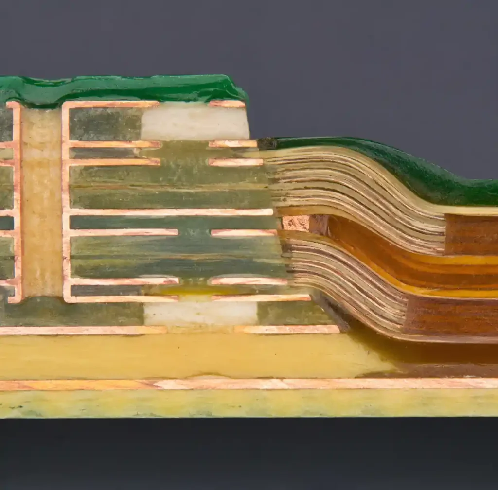
Unbalanced stackups cause warping, twisting, and reliability problems.
| Application | Rigid Section Layers | Flex Section Layers | Typical Stackup |
|---|---|---|---|
| Wearable devices | 4-6 layers | 1-2 layers | Signal + Ground/Power in flex |
| Medical instruments | 6-10 layers | 2-4 layers | Differential pairs + shields |
| Aerospace avionics | 10-20 layers | 2-4 layers | High-speed + power distribution |
| Industrial controls | 4-8 layers | 2 layers | Power + control signals |
Stackup principles:
- Use symmetrical layer construction (copper mirrors around center)
- Minimize layer count in flex sections (1-4 layers typical)
- Balance copper distribution to prevent bending bias
- Use thinner dielectric in flex sections (1-2mil polyimide vs 4-8mil FR4)
Mistake #7: Ignoring Coverlay Requirements
Coverlay is the protective dielectric layer on flex sections. Never use solder mask on flex sections—it cracks.
Coverlay specifications:
- Polyimide coverlay with acrylic adhesive: Standard, -55°C to +125°C
- Non-flow adhesive: High temperature, up to 200°C
- Bondply coverlay: Adhesiveless, thinnest option
Opening design: Coverlay openings should extend 0.1-0.2mm beyond pad edges to prevent solder wicking.
Mistake #8: Component Placement in Flex Areas
Never place components in areas designed to flex. All components must be located in rigid sections only.
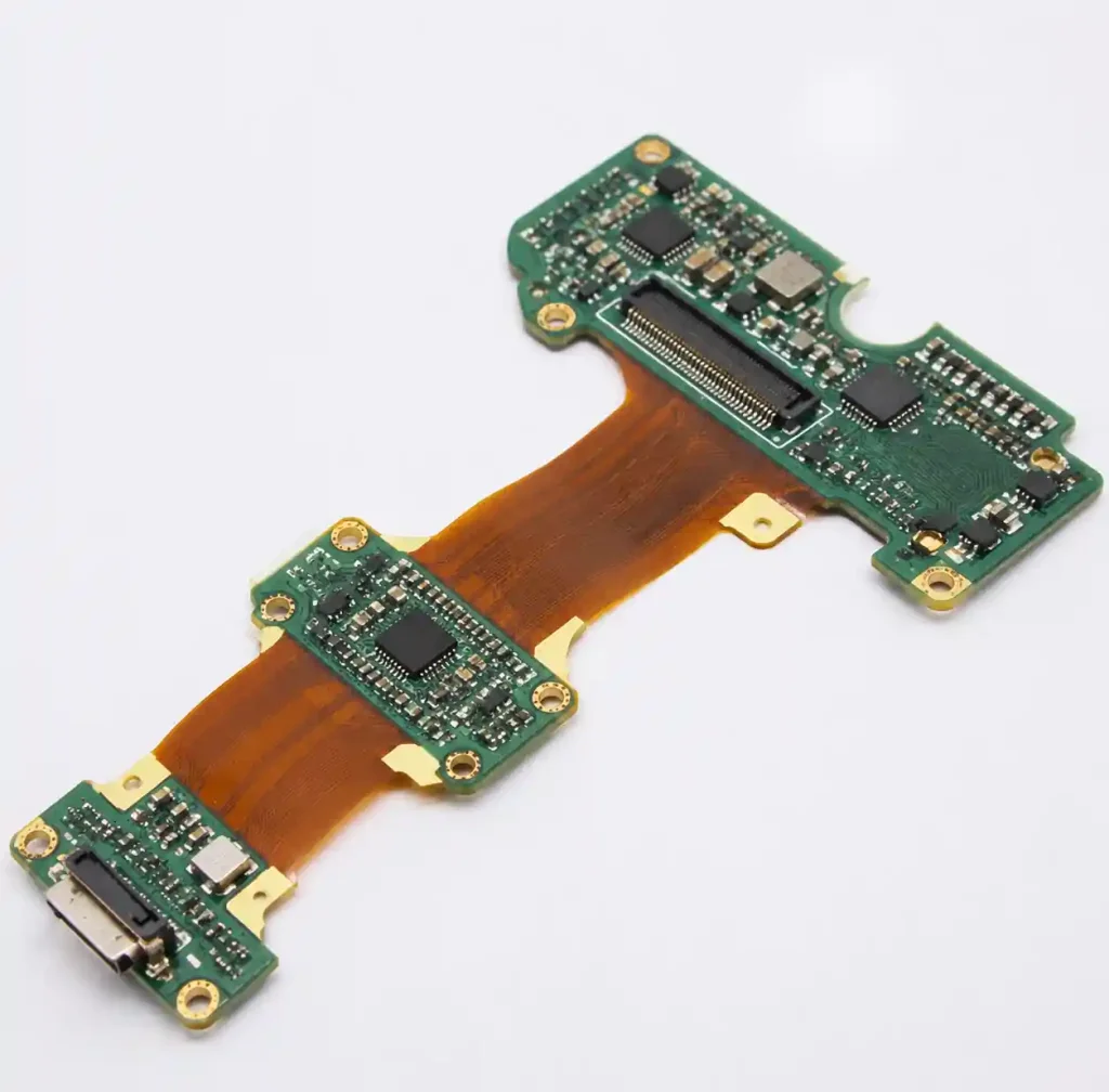
Guidelines:
- Keep all components minimum 3mm from rigid-flex boundaries
- Use rigid sections for high component density
- If a connector must be in flex area, add FR4 stiffener to create local rigid zone
- For dynamic flex, keep components 5mm from bend areas
Essential Design Guidelines
Material Selection:
- Flex substrate: Polyimide (Kapton) for -55°C to +200°C
- Adhesive: Acrylic for standard, non-flow for high-temp
- Rigid substrate: FR4 standard, high-Tg for lead-free assembly
Design Rules:
- Min trace width in flex: 0.075mm (3mil)
- Min trace spacing: 0.075mm (3mil)
- Min pad size: 0.5mm diameter for vias
- Annular ring: 0.075mm (3mil) minimum
- Rigid-to-flex transition: 2-3mm minimum

Design Verification Checklist
Before submitting design:
- [ ] Bend radius meets 10× thickness rule (dynamic) or 6× (static)
- [ ] No components in flex sections or within 3mm of transitions
- [ ] Stiffeners stop 1-2mm before bend areas
- [ ] ½oz or 1oz rolled-annealed copper in flex sections
- [ ] Traces perpendicular to bend axis
- [ ] No vias within bend radius areas
- [ ] Symmetrical copper distribution
- [ ] Coverlay openings extend 0.1-0.2mm beyond pads
Andwin Circuits provides comprehensive DFM review to identify issues before manufacturing.
FAQ
What is the minimum bend radius for rigid flex PCB?
10× total flex thickness for dynamic flexing, 6× thickness for static flex. A 0.2mm thick flex section requires 2.0mm dynamic or 1.2mm static bend radius.
Can I place components in the flexible section?
No. Components create rigid points that prevent flexing and cause solder joint failures. All components must be in rigid sections, minimum 3mm from rigid-flex transitions.
What copper weight should I use in flex sections?
½oz (17μm) or 1oz (35μm) rolled-annealed copper. Use ½oz for dynamic flex (1,000,000+ cycles) and 1oz for static flex. Never use 2oz+ in flex areas.
How many layers can rigid flex PCB have?
Up to 20+ total layers, with 4-20 layers in rigid sections and 1-4 layers in flex sections. Andwin Circuits manufactures up to 50 layers in rigid sections.
Why does rigid flex PCB cost more?
2-5× higher due to specialized materials, complex manufacturing with multiple lamination cycles, lower volumes, and longer lead times (15-25 days vs 7-10 days). Total system cost is often lower due to eliminated connectors and reduced assembly labor.

Conclusion
Rigid flex PCB design requires specialized knowledge beyond standard rigid PCB rules. Common mistakes—incorrect bend radius, wrong copper weight, poor via placement, improper trace routing, and components in flex areas—cause 70-80% of prototype failures.
Follow proper design guidelines: calculate bend radius at 10× flex thickness for dynamic applications, use ½oz to 1oz rolled-annealed copper, avoid vias and components in bend areas, route traces perpendicular to bends, and plan stiffener placement carefully.
If you need high-quality rigid flex PCB manufacturing with design review and DFM support, Andwin Circuits offers advanced capabilities up to 50 layers with fast turnaround in 15-20 days for prototypes, certified to ISO 9001, IATF 16949, and UL standards. Contact us today for custom rigid flex PCB solutions and competitive factory-direct pricing.