
PCB Design for IoT Devices: Size, Power, and Wireless Optimization
If you want to design successful IoT devices that achieve long battery life, reliable wireless connectivity, and compact form factors, then you will need to understand PCB miniaturization techniques, power optimization strategies, antenna integration methods, and EMI mitigation approaches.
The global IoT device market continues expanding rapidly, with connected devices expected to exceed 30 billion units by 2025. These devices demand PCBs that balance competing requirements: smaller size, lower power consumption, robust wireless performance, and cost-effectiveness. This technical guide covers proven strategies for optimizing PCB design across three critical dimensions of IoT device development.
Miniaturization Techniques for IoT PCBs
IoT devices increasingly require smaller form factors to fit constrained spaces in wearables, smart home devices, and industrial sensors.
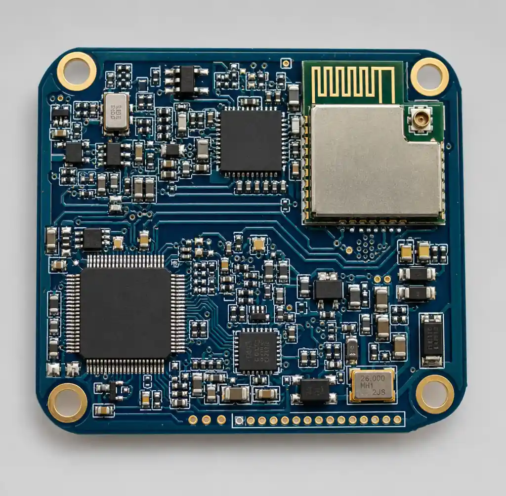
HDI (High-Density Interconnect) technology provides the foundation for miniaturized IoT PCBs. Laser-drilled microvias with diameters as small as 0.1mm allow routing between layers without consuming surface area, increasing routing density by 40-60% compared to traditional designs. You should specify HDI PCBs with 1+N+1 or 2+N+2 build-up structures when board size constraints require fine-pitch BGAs or component densities exceeding 80 components per square inch.
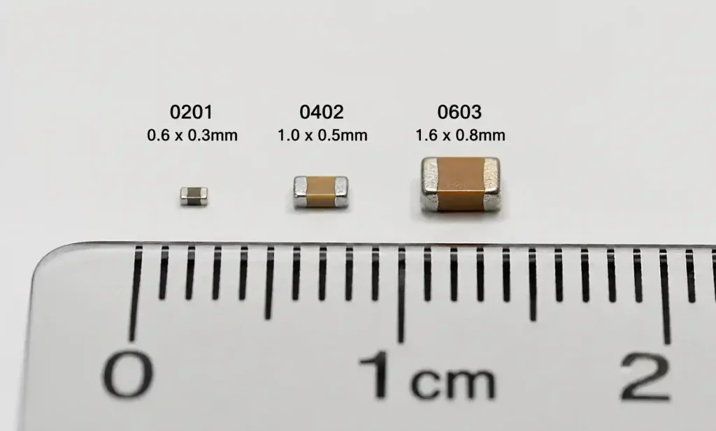
Component selection directly impacts board size. Modern IoT SoCs integrate MCU, wireless transceiver, and power management into single packages measuring 5mm × 5mm or smaller. Choosing 0201 (0.6mm × 0.3mm) passive components instead of 0402 sizes reduces board area by 30-50%. Rigid flex PCB construction eliminates connectors between board sections, reducing device volume by 15-25% for wearable fitness trackers and medical sensors.
Power Consumption Optimization
Battery life directly determines IoT device usability and maintenance costs. Optimizing power consumption extends operational life from months to years.
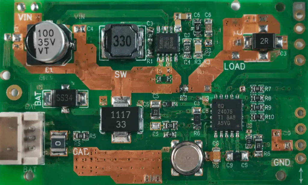
Switch-mode regulators (buck, boost, buck-boost) achieve 85-95% efficiency across wide load ranges. You should specify regulators with quiescent current below 10µA and burst mode operation for IoT devices spending most time in sleep states.
Power domain partitioning allows selective shutdown of unused circuitry. Separate power rails for MCU core, peripherals, sensors, and wireless modules enable fine-grained control. A typical IoT sensor operates the MCU for 100ms every 10 seconds, keeping wireless modules powered only during transmission. This duty cycling reduces average current from 20mA to under 100µA, extending coin cell battery life from weeks to years.
PCB trace resistance causes voltage drops in high-current paths. For traces carrying more than 500mA, calculate copper width using: Width(mm) = (Current(A) × 0.024) / (Thickness(oz) × Temp_Rise(°C)). A continuous ground plane provides low-impedance return paths, reducing ground bounce and power supply noise.
| Power Optimization Technique | Current Reduction | Implementation Complexity | Cost Impact |
|---|---|---|---|
| High-efficiency switching regulators | 30-50% vs linear | Medium | Low (+$0.50-2/unit) |
| Power domain partitioning | 60-80% average | High | Medium (design time) |
| Sleep mode optimization | 90-95% vs active | Medium | None |
| Voltage scaling | 20-40% per step | Medium | None |
| Sensor duty cycling | 70-85% average | Low | None |
Antenna Design and Integration
Wireless connectivity defines IoT functionality, making antenna design critical for reliable operation.
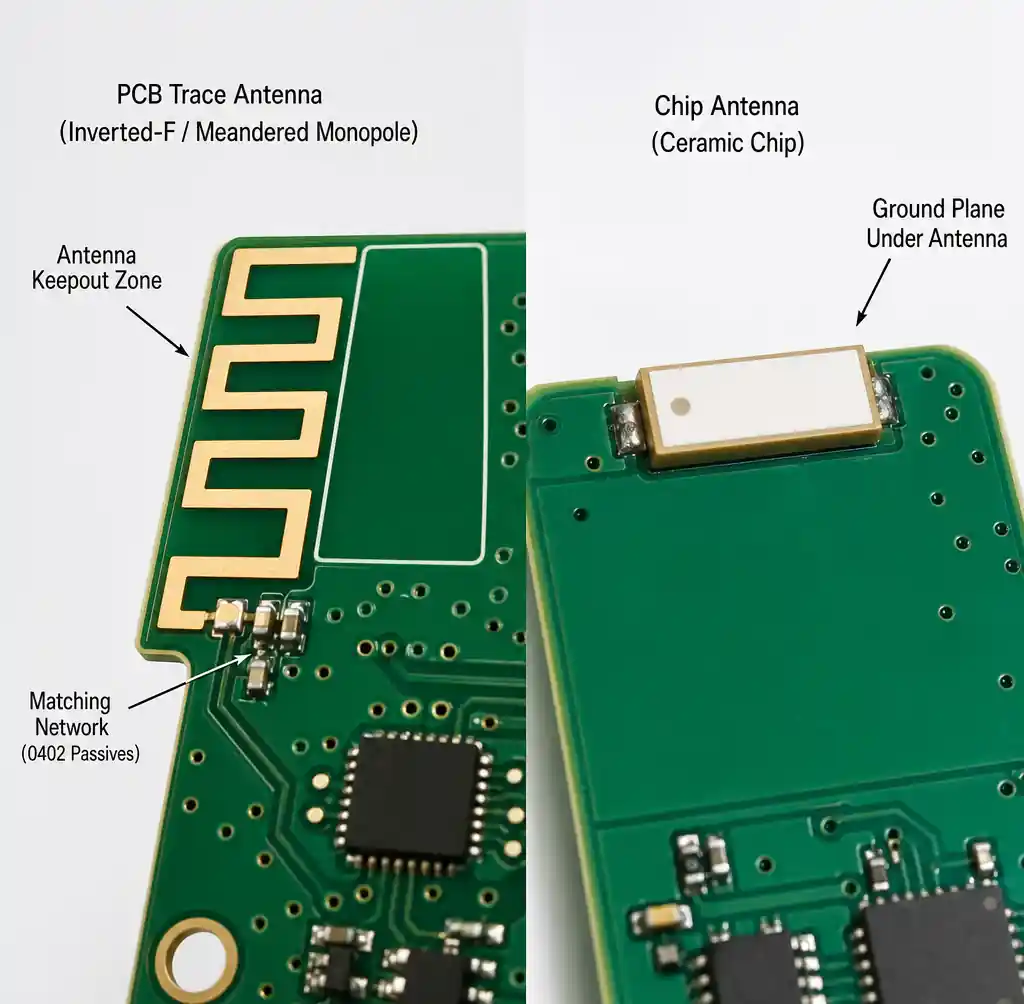
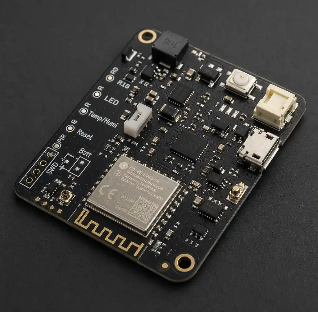
PCB trace antennas offer the lowest cost solution. Inverted-F antennas (IFA) and meandering monopoles work well for 2.4GHz applications, requiring 15-25mm board edge space with no ground plane underneath. You must maintain minimum 15mm clearance from metal components. PCB trace antennas achieve -1 to -3dBi gain, sufficient for short-range IoT applications under 30 meters.
The antenna keepout zone—area free of ground plane, traces, and components—extends at least 5mm around radiating elements for 2.4GHz designs. Violating keepout zones reduces antenna efficiency by 30-50%, directly reducing wireless range.
Chip antennas provide space-efficient solutions measuring 2mm × 3mm to 5mm × 7mm. Ground plane configuration affects resonant frequency; deviations shift center frequency by 50-150MHz. You should include provision for 0402 or 0201 matching components near the antenna feed point for post-layout tuning.
Battery Management Circuitry
Battery-powered IoT devices require protection circuits preventing damage from overcurrent, overvoltage, undervoltage, and temperature extremes.
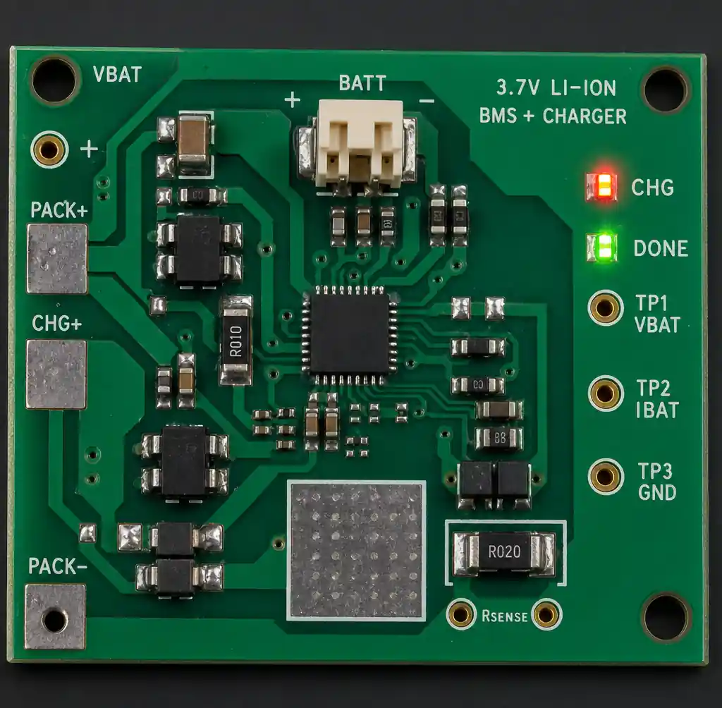
Lithium-ion and lithium-polymer batteries dominate IoT applications due to high energy density (150-250 Wh/kg) and operating voltage (3.0-4.2V). Battery management ICs from Texas Instruments (BQ series) provide constant-current/constant-voltage charging with thermal protection. Specify charging current at 0.5C to 1C rate for optimal cycle life.
Protection circuits disconnect battery during fault conditions. Overcurrent protection triggers at 150-200% of maximum rated current. Undervoltage lockout at 2.7-3.0V protects lithium cells from deep discharge. Overcharging above 4.25V causes thermal runaway risk; precision voltage references maintain ±1% charging voltage accuracy. Use 2mm minimum trace width for charging and discharge paths, with separate routing to prevent ground loops.
Wireless Module Integration
Pre-certified wireless modules accelerate IoT development by providing FCC, CE, and IC certified radio solutions.
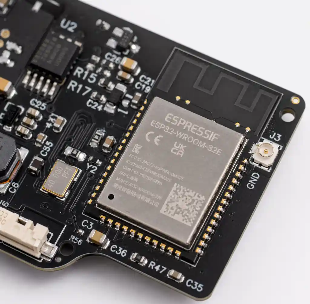
Module selection balances performance, power consumption, and cost. WiFi modules like ESP32 provide high data rates (up to 150Mbps) but consume 80-160mA during transmission. Bluetooth Low Energy modules achieve 5-15mA active current with 1-5µA sleep current, better suited for battery-powered sensors. LoRaWAN modules offer extreme range (2-15km) with ultra-low power consumption.
Most wireless modules specify 4-layer PCBs with uninterrupted ground plane directly under the module. This ground plane provides RF return path and heat sinking for power amplifiers. Avoid routing high-speed signals or power traces under RF modules, as coupling introduces noise degrading receiver sensitivity by 5-10dB.
EMI Considerations for 2.4GHz and 5GHz
Electromagnetic interference compromises wireless performance and regulatory compliance. IoT devices operating in 2.4GHz ISM and 5GHz bands face unique EMI challenges.
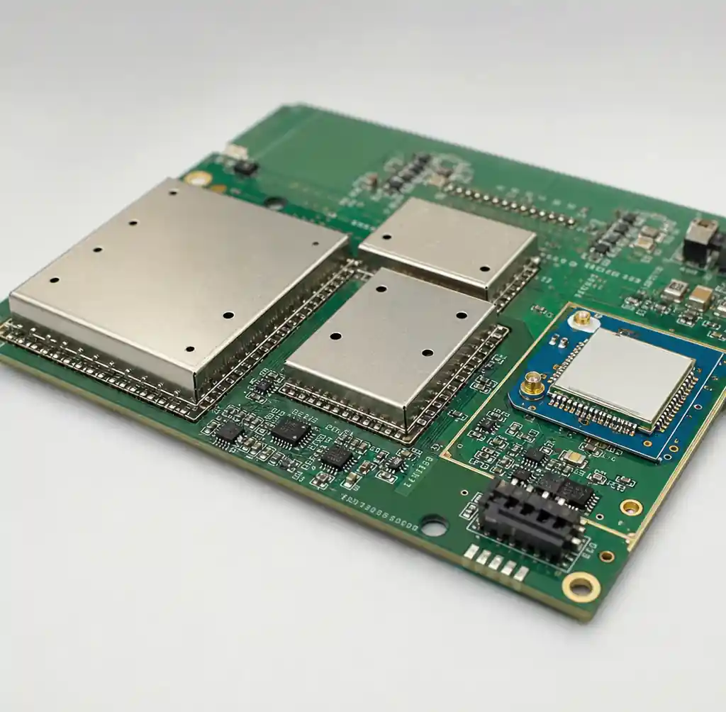
Switching power supplies generate broadband noise from 150kHz to above 1GHz. Buck converters with 1-2MHz switching frequencies create harmonics extending into 2.4GHz WiFi and Bluetooth bands. Specify switching regulators with spread-spectrum frequency modulation, reducing peak levels by 10-15dB. Locate switching regulators on opposite board side from wireless modules and separate by at least 30mm.
Shielding provides 20-40dB attenuation when properly implemented. Conformal metal shields over noise sources like switching regulators and clock oscillators prevent coupling to antenna. Use shield cans with compression gaskets contacting ground plane through multiple vias.
Crystal oscillators radiate harmonics that interfere with wireless receivers. A 26MHz crystal produces harmonics with the 93rd harmonic falling in 2.4GHz band. Place crystals away from antenna keepout zones, use series termination resistors (22-33Ω), and route clock traces as short differential pairs.
| EMI Source | Frequency Range | Mitigation Technique | Attenuation |
|---|---|---|---|
| Switching regulators | 1-100MHz + harmonics | Spread spectrum, shielding, filtering | 15-30dB |
| Digital buses (SPI, I2C) | 10-500MHz | Series termination, controlled impedance | 10-20dB |
| Crystal oscillators | Harmonics to 3GHz | Distance from antenna, routing control | 15-25dB |
| Display backlights | 20-100MHz | LC filtering, shielded cables | 20-30dB |
Cost Reduction Strategies
IoT device economics demand PCB designs balancing performance with manufactured cost.
Layer count significantly impacts PCB cost. A 4-layer board costs 40-60% less than 6-layer equivalent, with 2-layer designs another 30-40% cheaper. For consumer IoT devices, designing within 4-layer or 2-layer constraints substantially reduces unit costs.
Component consolidation reduces assembly costs. Selecting SoCs integrating MCU, wireless transceiver, and power management replaces 3-5 separate ICs, eliminating associated passives. System-in-Package modules simplify design and reduce board area by 30-50%.
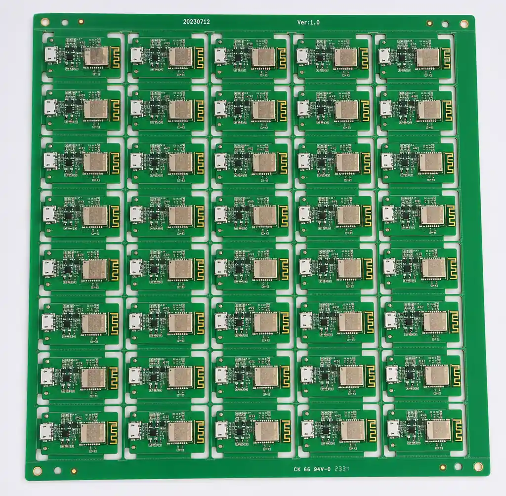
Panel utilization affects per-unit costs. Optimizing board dimensions to maximize pieces per panel directly reduces costs. A 50mm × 50mm board yields 40 pieces per panel, while 52mm × 52mm reduces to 35 pieces, increasing cost by 14%. Working with your PCB manufacturing partner identifies optimal dimensions.
Design for Manufacturing optimization prevents production issues. Minimum trace spacing of 0.15mm (6mil) accommodates standard processes without premium pricing. Andwin Circuits offers IoT and Wireless PCB manufacturing with cost optimization strategies including DFM review and component sourcing assistance.
IoT PCB Design Comparison
| PCB Technology | Size Reduction | Power Efficiency | Wireless Performance | Cost | Best Applications |
|---|---|---|---|---|---|
| Standard 2-layer | Baseline | Good | Good | Lowest | Simple sensors, prototypes |
| 4-layer with HDI | 30-40% smaller | Excellent | Excellent | Medium | Smart home, wearables |
| 6-layer HDI | 50-60% smaller | Excellent | Excellent | High | Medical devices, high-performance IoT |
| Rigid-flex | 15-25% volume reduction | Excellent | Good | Highest | Wearables, curved enclosures |
| Flex PCB | Maximum flexibility | Good | Fair-Good | Medium-High | Ultra-compact sensors |
FAQs
What layer count is best for IoT PCB designs?
Most IoT devices use 4-layer PCBs providing good compromise between cost, size, and performance. The stackup includes top signal, ground plane, power plane, and bottom signal layer. This supports controlled impedance for wireless RF traces while maintaining reasonable costs. Simple sensors may use 2-layer boards, while complex designs require 6-8 layers.
How do I reduce power consumption in my IoT PCB design?
Choose MCUs and wireless modules with low sleep current (under 10µA). Implement power domain partitioning with load switches allowing selective shutdown. Use high-efficiency switching regulators (85-95% efficiency). Design for duty cycling where sensors and wireless modules operate briefly then return to sleep, reducing average current by 80-90%.
Can I use a 2-layer PCB for WiFi or Bluetooth IoT devices?
Yes, but with limitations. 2-layer boards can support 2.4GHz wireless with proper ground plane coverage (70-80% of bottom layer), controlled impedance traces, and adequate antenna keepout zones. However, 4-layer construction significantly improves wireless performance by providing better RF return paths and noise isolation.
What antenna type should I use for my IoT device?
PCB trace antennas offer lowest cost for devices with available board space (15-25mm edge area). Chip antennas work well for space-constrained designs but require careful layout. External antennas with U.FL connectors provide best performance for metal enclosures. Most consumer IoT devices under 30m range use PCB trace or chip antennas.
How far should I place my switching regulator from my wireless module?
Maintain minimum 30mm separation between switching regulators and wireless modules. Place regulators on opposite board side when possible, with solid ground plane between for shielding. If same-side placement is unavoidable, use metal shields over regulators. Distance, shielding, and filtering together achieve 30-40dB isolation.
What PCB material should I use for IoT devices?
Standard FR-4 material works well for most IoT applications operating below 2.5GHz and in temperature ranges of -20°C to +85°C. FR-4 provides good electrical properties and lowest cost. For high-frequency designs above 3GHz, consider Rogers RO4003C in RF sections only.
Conclusion
Successful IoT PCB design requires balancing size, power efficiency, wireless performance, and cost. HDI PCB technology achieves 30-60% size reduction, while power domain partitioning extends battery life from weeks to years. Proper antenna integration, EMI mitigation, and grounding ensure reliable wireless connectivity. Strategic cost optimization through layer count selection and DFM principles maintains competitive pricing.
Andwin Circuits offers advanced manufacturing capabilities including HDI PCB up to 50 layers, rigid-flex solutions, and specialized RF designs with fast delivery in 7 days. Our facility is certified to ISO 9001 and UL standards, ensuring superior quality for consumer electronics, industrial monitoring, and wireless communication applications worldwide.
Contact us today for custom IoT PCB solutions and competitive factory-direct pricing.