
High Voltage PCB Design: Creepage, Clearance, and Safety Requirements
High voltage PCB failures account for 18% of power electronics recalls, with inadequate creepage and clearance cited as primary causes in industrial equipment, EV charging systems, and medical devices. A single arc-over can destroy components, create fire hazards, and expose manufacturers to liability claims exceeding millions of dollars.
Here is what most design guides skip: creepage and clearance are not suggestions from a handbook. They are calculated values derived from working voltage, pollution degree, material group, and altitude per IPC-2221 and IEC 60664-1. This article shows how to calculate both distances correctly, why PCB material CTI rating matters, and how high voltage PCB design is validated for safety compliance.
What Are Creepage and Clearance?
Creepage is the shortest path along the PCB surface between two conductive parts. Clearance is the shortest distance through air between those same points. Both prevent electrical breakdown, but they protect against different failure modes.
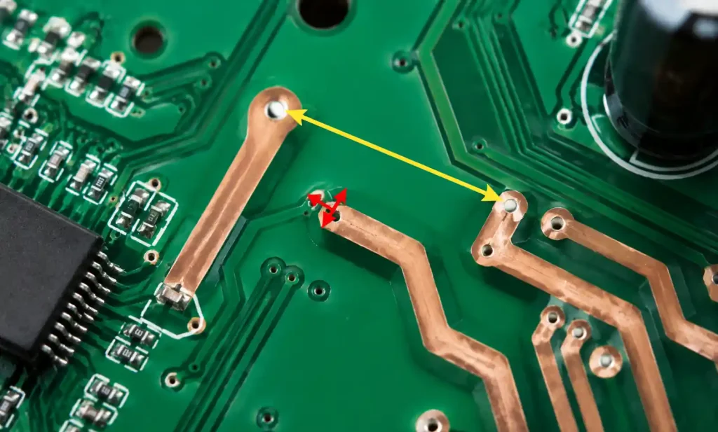
Clearance prevents arc-over through air, which depends on voltage and altitude. Creepage prevents tracking across contaminated surfaces, which depends on voltage, material properties, and environmental pollution. You cannot substitute one for the other because surface contamination creates conductive paths that air gaps do not experience.
| Parameter | Creepage | Clearance |
|---|---|---|
| Path | Along PCB surface | Through air |
| Failure mode | Surface tracking, carbonization | Electric arc, corona discharge |
| Key factors | Voltage, CTI rating, pollution degree | Voltage, altitude, transient overvoltage |
| Design impact | PCB layout, slots, grooves | Component spacing, enclosure gaps |
| Typical requirement | 2-10mm for 300-600Vac | 1.5-6mm for 300-600Vac |
For a 400Vac system at sea level with Pollution Degree 2, IEC 60664-1 requires 3.2mm creepage and 1.6mm clearance. Creepage is always equal to or greater than clearance because surface paths accumulate contamination over time.
IPC-2221 vs IEC 60664-1 Standards
Two standards govern high voltage PCB spacing, and they produce different results. IPC-2221 is the North American PCB design standard used for UL certification. IEC 60664-1 is the international low-voltage equipment standard used for CE marking and global markets.
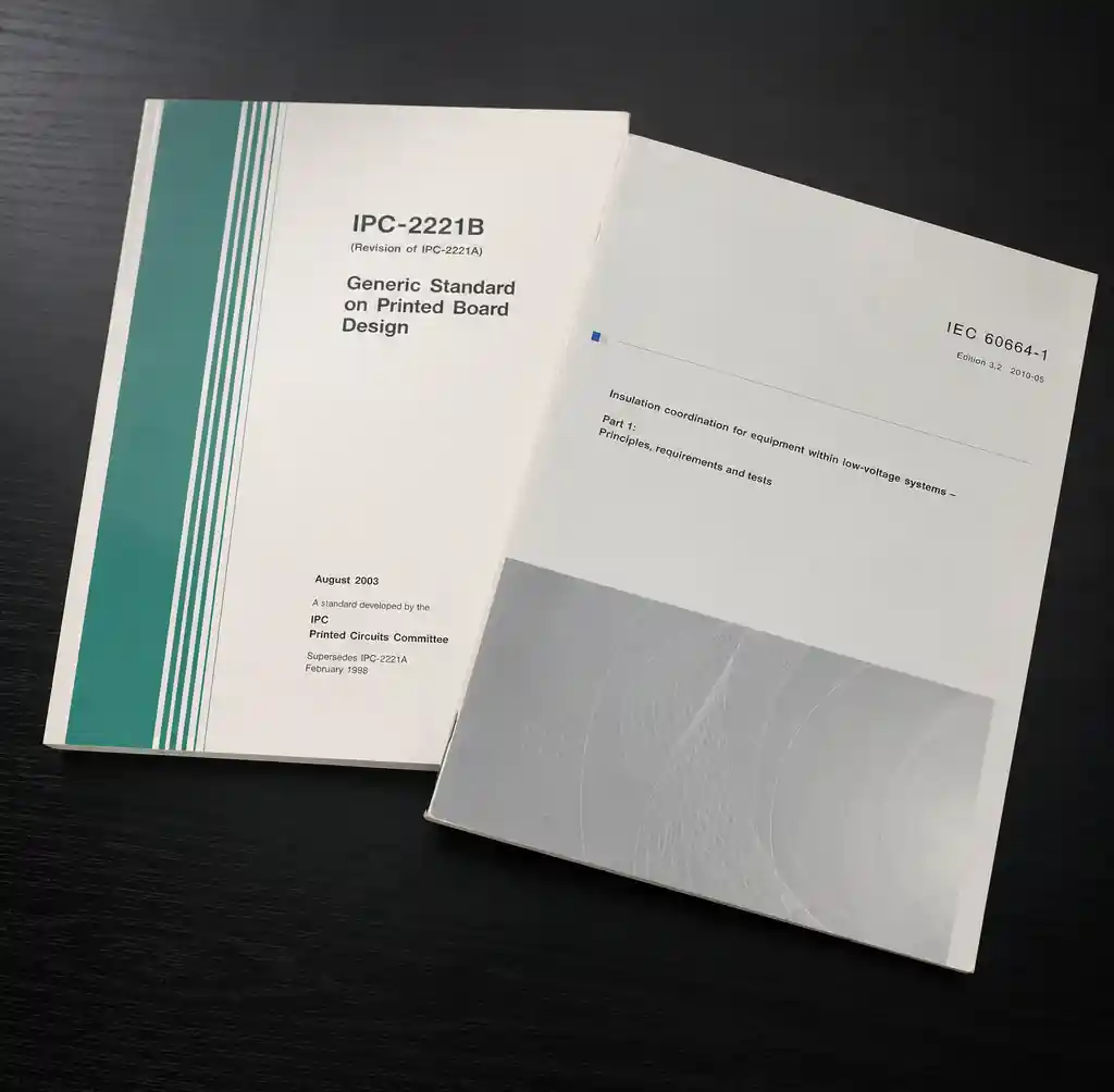
IPC-2221 bases creepage on voltage and coating type, with values ranging from 0.1mm per volt (uncoated, external conductors) to 0.64mm per volt (coated, internal conductors). For 300V, uncoated external traces require 30mm creepage, which is impractical for most designs.
IEC 60664-1 uses lookup tables that factor working voltage, insulation type (functional, basic, reinforced), pollution degree (1-4), and material group (I, II, IIIa, IIIb). For the same 300V system with reinforced insulation and Pollution Degree 2, IEC requires only 4mm creepage—seven times less than IPC-2221 uncoated external.
| Standard | Basis | Typical creepage (400Vac) | Use case |
|---|---|---|---|
| IPC-2221 | Voltage × factor | 40mm (uncoated) / 2.6mm (coated) | UL cert, North America |
| IEC 60664-1 | Voltage + pollution + CTI | 3.2-6.4mm (depends on insulation type) | CE mark, global markets |
| IEC 61010 | Medical, lab equipment | Per IEC 60664-1 + category | Medical, measurement |
| IEC 60950 | IT equipment (obsolete) | Replaced by IEC 62368-1 | Legacy designs |
Most commercial designs follow IEC 60664-1 because it produces practical spacing for modern high-density boards. UL certification still references IPC-2221, but UL allows IEC 60664-1 values with proper material documentation and CTI test reports.
Creepage Distance Calculation
Creepage distance is calculated using IEC 60664-1 Table 4 (functional and basic insulation) or Table 5 (reinforced insulation). The working voltage is the RMS or DC voltage present during normal operation, not peak or transient values.
For pollution degree selection: Degree 1 is clean environments (sealed enclosures, filtered air), Degree 2 is normal indoor conditions with occasional condensation, Degree 3 is industrial environments with conductive dust, and Degree 4 is outdoor exposure with continuous conductivity.

Calculation example for 230Vac system, reinforced insulation, Pollution Degree 2, Material Group IIIb (CTI 175-249):
- Working voltage: 230Vac
- Insulation type: Reinforced (two-fault protection)
- Pollution Degree: 2 (normal indoor)
- Material Group: IIIb (FR4 with CTI 175-249)
- IEC 60664-1 Table 5: 4.0mm minimum creepage
If the same circuit uses Material Group IIIa (CTI 100-174), the required creepage increases to 5.5mm. This 38% increase shows why PCB material selection matters early in the design phase.
For altitudes above 2000m, apply a correction factor because air density decreases. At 3000m, multiply clearance by 1.14; at 4000m, by 1.29. Creepage values do not change with altitude because surface tracking is independent of air pressure.
Clearance Distance Calculation
Clearance is calculated using IEC 60664-1 Table 2 for transient overvoltage category and Table 3 for altitude correction. Transient overvoltage categories are: CAT I (protected electronics), CAT II (appliances fed from mains), CAT III (fixed installation distribution), and CAT IV (origin of installation, utility connection).
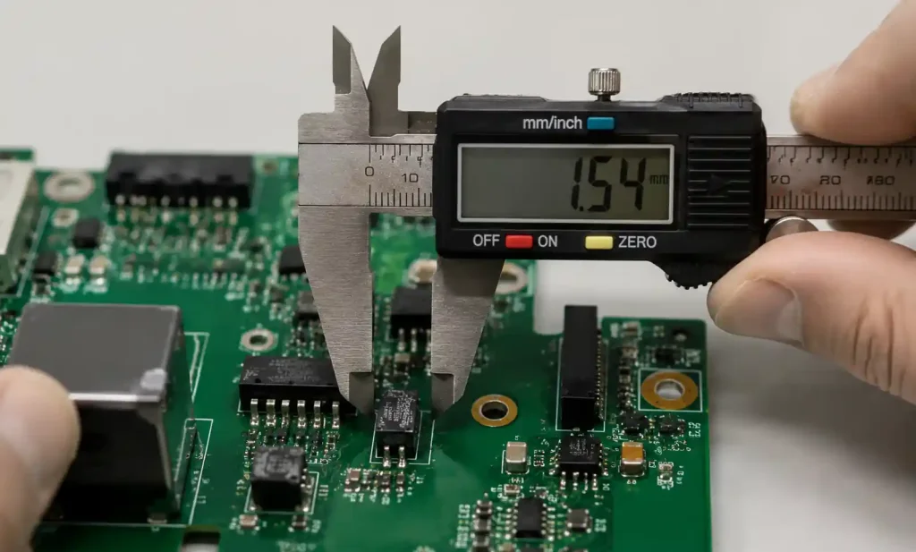
Clearance depends on peak working voltage plus expected transients. For a 230Vac CAT II system (325V peak), IEC 60664-1 requires 1.5mm basic insulation clearance. Reinforced insulation doubles this to 3.0mm.
Clearance example for 400Vdc system, CAT III, 2500m altitude, reinforced insulation:
- Working voltage: 400Vdc
- Overvoltage category: CAT III (4kV transient expected)
- IEC 60664-1 Table 2: 2.5mm base clearance for reinforced
- Altitude correction at 2500m: 1.10×
- Final clearance required: 2.5mm × 1.10 = 2.75mm
High voltage DC systems above 500V require additional consideration because DC voltage does not have a zero crossing to extinguish arcs. Use the DC voltage directly in IEC tables without RMS conversion.
Material CTI Rating and Pollution Degree
Comparative Tracking Index (CTI) measures a material’s resistance to surface tracking under electrical stress and contamination. It is tested per IEC 60112 by applying voltage across two electrodes on the material surface while dripping contaminated water solution between them. The CTI value is the maximum voltage that does not cause tracking failure after 50 drops.
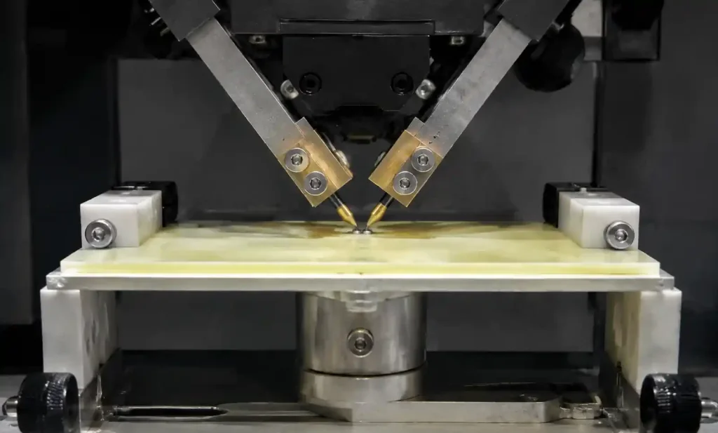
Standard FR4 laminate typically achieves CTI 175-249 (Material Group IIIb). High-CTI materials with filler additives reach CTI 250-399 (Group IIIa) or CTI 400-599 (Group II). These materials cost 20-40% more but allow tighter spacing in Pollution Degree 2 and 3 environments.
| Material Group | CTI Range | Typical materials | Creepage multiplier (vs Group I) |
|---|---|---|---|
| Group I | CTI 600+ | High-grade ceramic, PTFE | 1.0× (baseline) |
| Group II | CTI 400-599 | High-CTI FR4, polyimide | 1.25× |
| Group IIIa | CTI 250-399 | Modified FR4, some epoxy | 1.6× |
| Group IIIb | CTI 175-249 | Standard FR4, phenolic | 2.0× |
For a 300V system in Pollution Degree 2, Material Group I requires 2.0mm creepage while Group IIIb requires 4.0mm—double the spacing. This difference directly impacts board size and cost in power electronics PCB applications.
Conformal coating does not improve CTI rating but reduces pollution degree accumulation. A coated board in a Pollution Degree 3 environment can be designed to Pollution Degree 2 values if the coating is specified and tested per IPC-HDBK-830.
PCB Design Techniques for High Voltage
High voltage PCB layout requires specific techniques beyond standard spacing rules. These methods have been validated in industrial power supplies, EV charging systems, and medical equipment at Andwin Circuits for over 15 years.
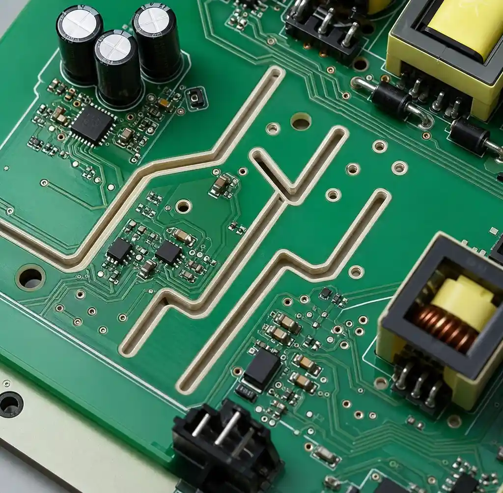
Slots and grooves: Routing a slot perpendicular to the high voltage path forces creepage to travel around the slot, extending the surface distance without increasing board width. A 2mm wide slot adds 4mm to creepage path (2mm down, 2mm up). Slots must be at least 1mm wide and extend fully through the board to be effective per IPC-2221.
Guard traces and rings: A grounded trace between high and low voltage areas intercepts leakage current and prevents tracking. The guard trace must connect to earth ground, not floating, and must maintain proper creepage from both the high voltage and low voltage sides.
Keep-out zones: Define minimum spacing in your PCB design CAD library as a design rule. For 400V systems, create a 5mm exclusion zone around high voltage traces that blocks routing, vias, and copper pours. This prevents accidental violations during layout changes.
Layer assignment: Place high voltage traces on outer layers where contamination is visible and repairable. Internal layers accumulate moisture through board edges and vias, creating invisible tracking paths. If high voltage must route internally, ensure controlled impedance PCB stackup with low-moisture laminates.
Thermal relief and solder mask: Do not rely on solder mask for electrical spacing. Solder mask typically withstands only 500-1000V breakdown and is not rated insulation. Maintain full creepage and clearance in bare copper, then apply mask as physical protection only.
Safety Certification Requirements
High voltage PCBs require third-party certification before market release in most countries. The certification body tests actual boards under worst-case conditions including humidity, temperature cycling, and dielectric withstand voltage tests.
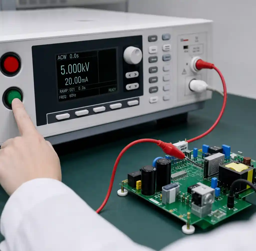
UL 60950-1 / UL 62368-1 (North America): IT and audio/video equipment. Requires hipot testing at 2× working voltage + 1000V for 60 seconds. PCB must show no breakdown, flashover, or tracking. UL inspects production quarterly to verify ongoing compliance.
IEC 60950-1 / IEC 62368-1 (International): Same scope as UL but used for CE marking in Europe and other global markets. Testing requirements align with UL but acceptance criteria may differ for medical and industrial categories.
IEC 61010 (Measurement and lab equipment): Covers oscilloscopes, power supplies, and test equipment. Requires reinforced insulation between mains and user-accessible circuits with extended creepage distances for Pollution Degree 2. IC test boards and high-voltage measurement equipment follow this standard.
IEC 60601 (Medical equipment): Most stringent requirements with patient safety as primary concern. Requires 2× MOPP (Means of Patient Protection) isolation, which doubles the reinforced insulation spacing. Medical device PCBs often need 8-10mm creepage for 230Vac systems.
For automotive PCB applications, ISO 7637 defines transient immunity requirements and LV 124 specifies voltage ranges. Electric vehicle charging equipment follows IEC 61851 with additional spacing for DC voltages up to 1000V.
Common Design Mistakes
From production failure analysis and certification testing at Andwin Circuits, these errors cause 80% of high voltage PCB safety failures.
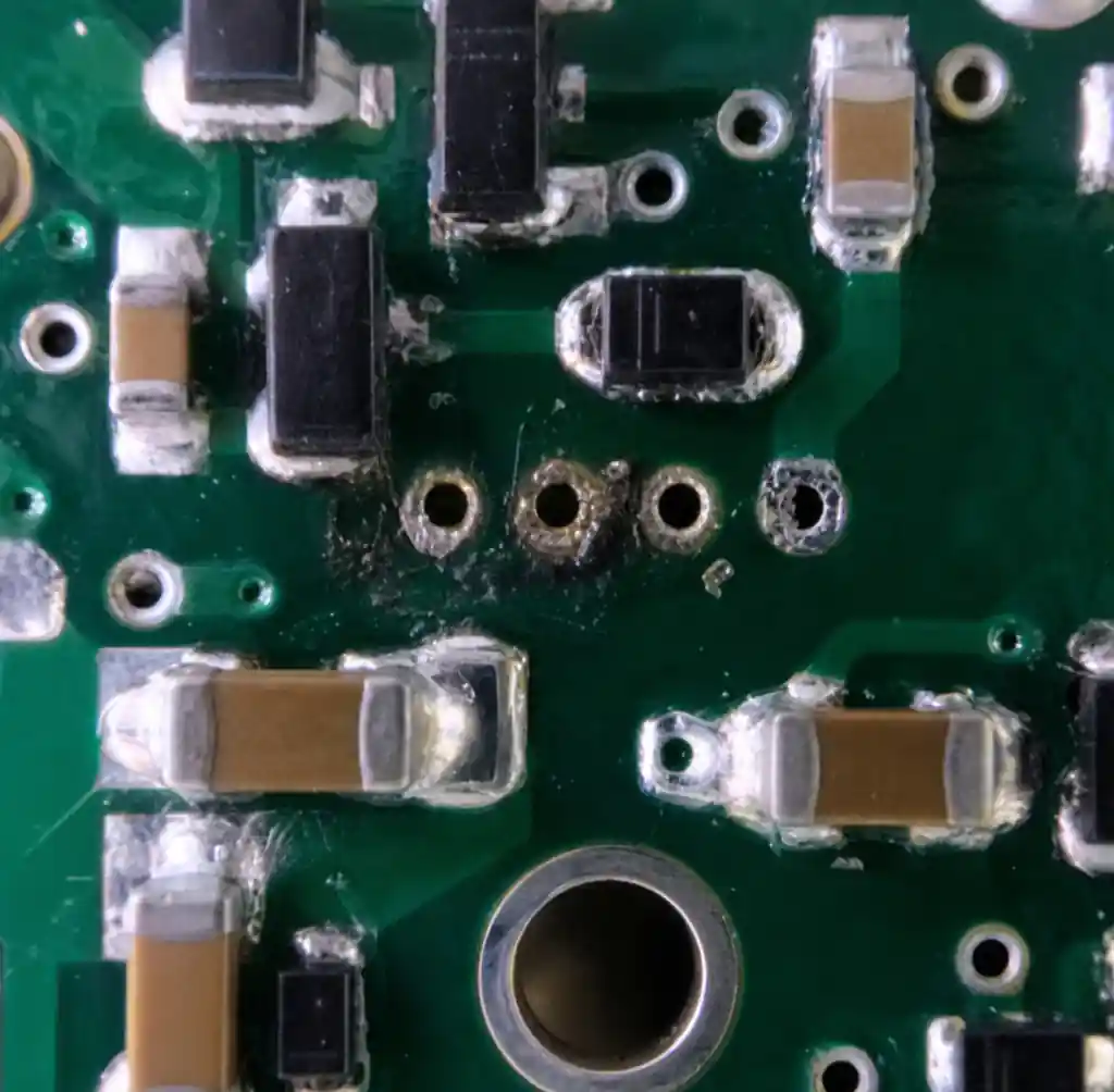
Mistake 1: Measuring clearance through components, not around them. Clearance must account for component body, lead spacing, and solder fillet dimensions. A component placed between high and low voltage must have its body height added to the air gap calculation.
Mistake 2: Ignoring solder mask dams. Solder mask between pads can bridge during reflow if spacing is insufficient. Maintain at least 0.1mm mask dam or specify no mask between high voltage pads in your PCB assembly documentation.
Mistake 3: Violating spacing at via locations. A via near a high voltage trace creates a clearance violation if the via connects to ground or low voltage on another layer. Check all layers, not just the visible routing layer.
Mistake 4: No altitude derating documentation. If your product ships globally, it must meet clearance requirements at 2000m minimum per IEC standards. Document the maximum operating altitude in specifications.
Mistake 5: Using generic FR4 in harsh environments. Standard CTI 175 material fails in Pollution Degree 3 environments with condensation and dust. Specify high-CTI material (CTI 250+) for industrial and outdoor applications, or accept the larger creepage spacing penalty.
FAQs
What is the difference between functional, basic, and reinforced insulation?
Functional insulation is required for circuit operation only, with no safety function. Basic insulation provides single-fault protection (one layer of insulation). Reinforced insulation provides two-fault protection equivalent to two layers of basic insulation. Medical and mains-powered equipment typically requires reinforced insulation between AC input and user-accessible circuits.
Can I reduce creepage by applying conformal coating?
Conformal coating allows you to design for one pollution degree lower (Degree 3 to Degree 2) but does not reduce the calculated creepage distance. You must still maintain the full calculated spacing in bare copper. The coating provides additional protection against moisture and contamination but is not rated insulation per IEC standards.
How do I calculate spacing for DC voltages?
Use the DC voltage value directly in IEC 60664-1 tables without RMS conversion. DC systems do not benefit from zero-crossing arc extinction, so clearance requirements are often more stringent than AC at the same voltage level. For pulsed DC or PWM waveforms, use the peak voltage value.
What happens if my PCB violates clearance during vibration?
Dynamic clearance under vibration, shock, and thermal expansion must be considered in mechanical design. IEC 60664-1 requires that clearance distances are maintained under all operating conditions including maximum deflection. For rigid flex PCB designs, calculate bend radius effects on conductor spacing.
Do slots need to be plated or can they be routed?
Slots can be unplated routed cutouts. Plating the slot walls does not reduce effectiveness as long as the plating connects to neither high nor low voltage traces. The slot increases creepage by forcing surface current to travel down and up the slot walls regardless of plating.
What voltage defines “high voltage” for PCB design purposes?
IEC 60664-1 applies to equipment with working voltages up to 1000Vac or 1500Vdc. Below 50Vac or 120Vdc is considered ELV (Extra Low Voltage) with reduced spacing requirements. For PCB designers, any voltage above 50V requires formal creepage and clearance calculations rather than standard DRC minimum spacing rules.
Conclusion
High voltage PCB design requires calculated creepage and clearance distances per IEC 60664-1 and IPC-2221, with values determined by working voltage, insulation type, pollution degree, material CTI rating, and altitude. Proper spacing prevents arc-over, surface tracking, and safety certification failures that cause product recalls and liability exposure.
If you need high-quality PCB manufacturing for high voltage applications, Andwin Circuits offers advanced capabilities up to 50 layers with IPC Class 3 workmanship and UL certification. Our facility is certified to ISO 9001, IATF 16949, and IEC standards, ensuring superior quality and safety compliance for power electronics, medical, industrial, and automotive products worldwide.
Contact us today for custom PCB solutions with proper high voltage spacing design review, CTI-rated materials selection, and certification support for your safety-critical applications.