
PCB Manufacturing Defects: Lamination Voids and Delamination Prevention
Lamination defects account for 15-25% of multilayer PCB failures in high-reliability applications, with delamination and void formation being the leading causes of field returns in automotive, aerospace, and medical electronics. Understanding root causes and implementing prevention strategies is critical for hardware engineers working on complex multilayer designs.
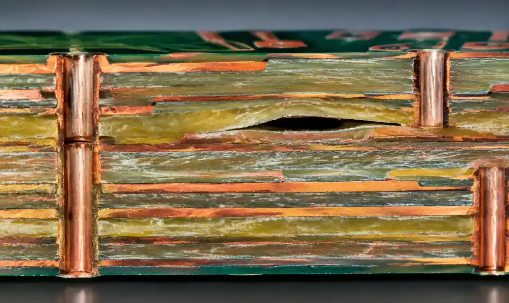
What Are Lamination Voids and Delamination?
Lamination voids are unfilled spaces between PCB layers where bonding resin fails to completely wet copper and glass fiber surfaces during lamination. These voids typically range from 10 microns to several millimeters, forming when air, moisture, or contamination prevents proper resin flow under heat and pressure.
Delamination is the physical separation of bonded layers within the PCB structure, occurring between base material layers, between copper foil and substrate, or between solder mask and board surface. This separation compromises mechanical strength and electrical insulation, creating failures that develop during thermal cycling or environmental stress.
Root Causes of Lamination Voids
Moisture Contamination
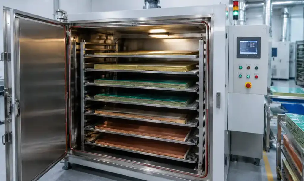
Absorbed moisture in prepreg and core materials is the primary cause of void formation. FR4 laminates absorb 0.1-0.3% moisture by weight at 23°C and 50% relative humidity. During lamination, this moisture vaporizes above 170°C, creating vapor pockets that push resin away from bonding surfaces.
IPC-4101 specifies baking FR4 materials at 105-120°C for 2-4 hours to reduce moisture below 0.05% before lamination. High-Tg materials requiring lamination above 200°C need longer bake cycles due to lower moisture permeability.
Surface Contamination
Copper oxide formation, fingerprint oils, photoresist residue, and particulate contamination prevent proper resin-to-copper wetting. Brown oxide and black oxide treatments provide 2-4 micron peak-to-valley roughness, but contamination blocks resin penetration.
Proper surface preparation requires alkaline cleaning followed by micro-etching to remove 1-2 microns of copper. Plasma cleaning further reduces contact angle from 80-90° to below 20°, improving resin wetting. Time between oxide treatment and lamination should not exceed 24-48 hours.
Inadequate Lamination Pressure
Insufficient pressure prevents complete resin flow and air evacuation. Standard multilayer lamination requires 300-400 PSI (2.1-2.8 MPa), but high-layer-count boards may need 400-500 PSI for proper consolidation.
Pressure must be applied gradually during heat-up to allow resin flow before gelation. Rapid pressure traps air and gases that cannot escape through viscous resin. Press cycles typically hold 50-100 PSI during heat-up, then increase to full pressure after reaching 150-170°C where resin viscosity is lowest.

Resin Flow Issues
Prepreg resin content directly impacts void formation risk. Standard FR4 prepreg contains 42-48% resin by weight, but multilayer stackups with fine-line circuitry need higher resin content (48-52%) to fill gaps between traces and ensure complete bonding.
Resin flow during lamination depends on viscosity, which decreases with temperature. At 170°C, epoxy resin viscosity drops to 50-100 poise, allowing flow into micro-roughened surfaces. Insufficient heating prevents this low-viscosity window, leaving voids in high-surface-area regions.
Delamination Mechanisms
Thermal Stress and CTE Mismatch
Coefficient of thermal expansion mismatch between copper (17 ppm/°C) and FR4 substrate (14-17 ppm/°C in XY, 50-70 ppm/°C in Z-axis) creates stress during thermal cycling. Each reflow cycle at 260°C generates shear stress at copper-substrate interfaces, weakening the resin bond.
High-Tg laminates (Tg 170-180°C) maintain better stability than standard FR4 (Tg 130-140°C) during assembly. IPC-4101 requires Z-axis CTE below 3.5% for high-reliability applications to minimize stress through multiple assembly cycles.
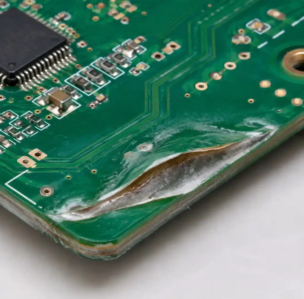
Moisture-Induced Delamination
Absorbed moisture in assembled PCBs causes explosive delamination during reflow. When moisture-saturated FR4 reaches 260°C, water vapor pressure exceeds 40 atmospheres, forcefully separating layers at weak interfaces.
IPC-J-STD-033 defines moisture sensitivity levels and pre-bake requirements. Level 3 boards (moisture >0.2%) require 24-hour bake at 125°C before reflow to prevent popcorning. This is critical in lead-free assembly where peaks reach 260°C versus 240°C for tin-lead.
Press Cycle Optimization
| Parameter | Standard Multilayer | High-Layer HDI | Impact on Voids |
|---|---|---|---|
| Ramp Rate | 2-3°C/min | 1.5-2°C/min | Slower allows outgassing |
| Peak Temperature | 185-195°C | 200-220°C | Higher reduces viscosity |
| Dwell Time | 60-90 min | 90-120 min | Extended ensures cure |
| Pressure | 300-400 PSI | 400-500 PSI | Higher evacuates air |
| Cooling Rate | <3°C/min | <2°C/min | Controlled prevents stress |
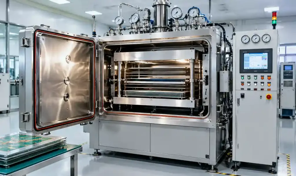
Vacuum-assisted lamination reduces void formation by evacuating the stack to 0.1-1 torr before applying pressure. This removes trapped air and lowers moisture vaporization temperature. Aerospace and medical PCB manufacturers commonly use vacuum lamination for Class 3 boards.
C-SAM Inspection and Detection
Scanning acoustic microscopy (C-SAM) is the primary non-destructive method for detecting lamination voids and delamination. This technique uses ultrasonic waves at 15-230 MHz to identify density changes at interfaces, revealing voids as low-density regions that reflect acoustic signals differently.
C-SAM detects voids as small as 10-15 microns and delaminations less than 1 micron thick, far beyond visual inspection capability. The technique scans through PCB thickness, generating layer-by-layer images showing void location, size, and distribution. Red or bright areas indicate poor bonding or air gaps.

Inspection Acceptance Criteria
IPC-6012 Class 3 limits acceptable void size and density in critical areas. Individual voids must not exceed 5% of pad or trace area, and total void area cannot exceed 25% in any bonding interface. These criteria apply to aerospace, medical, and military applications.
For Class 2 consumer electronics, criteria are less stringent, allowing individual voids up to 10% of feature size and 30% total void area. Automotive applications should follow IATF 16949 quality requirements, which align with Class 3 standards due to safety-critical nature.
Prevention Strategies
Design for Manufacturability
Circuit design impacts lamination void risk. Dense copper areas create resin-starved regions because resin cannot flow into small gaps. Designs with less than 4 mil (100 micron) spacing need higher resin content prepreg or additional bonding layers.
Large copper pours should include thermal relief and thief patterns to balance copper distribution. Unbalanced copper between layers creates differential thermal expansion promoting delamination. Target 30-50% copper coverage per layer for optimal results.
Process Control and Monitoring
Real-time monitoring prevents void formation before it occurs. Modern presses record temperature, pressure, and vacuum throughout cycles, allowing correlation between variations and C-SAM results. Statistical process control identifies parameter drift before yield impact.
Critical control points include prepreg moisture content (<0.05% before lamination), oxide treatment thickness (0.8-1.2 microns), and post-oxide storage time (<24 hours). Deviation increases void risk exponentially—a 0.1% moisture increase can double void occurrence.
Rogers/FR4 Mixed Dielectric Challenges
Mixed dielectric stackups using high-frequency materials like Rogers RO4350B with FR4 present unique delamination risks. Rogers laminates have lower CTE (10-12 ppm/°C) and different resin chemistry than FR4, creating weak bonding interfaces and thermal stress at material transitions.
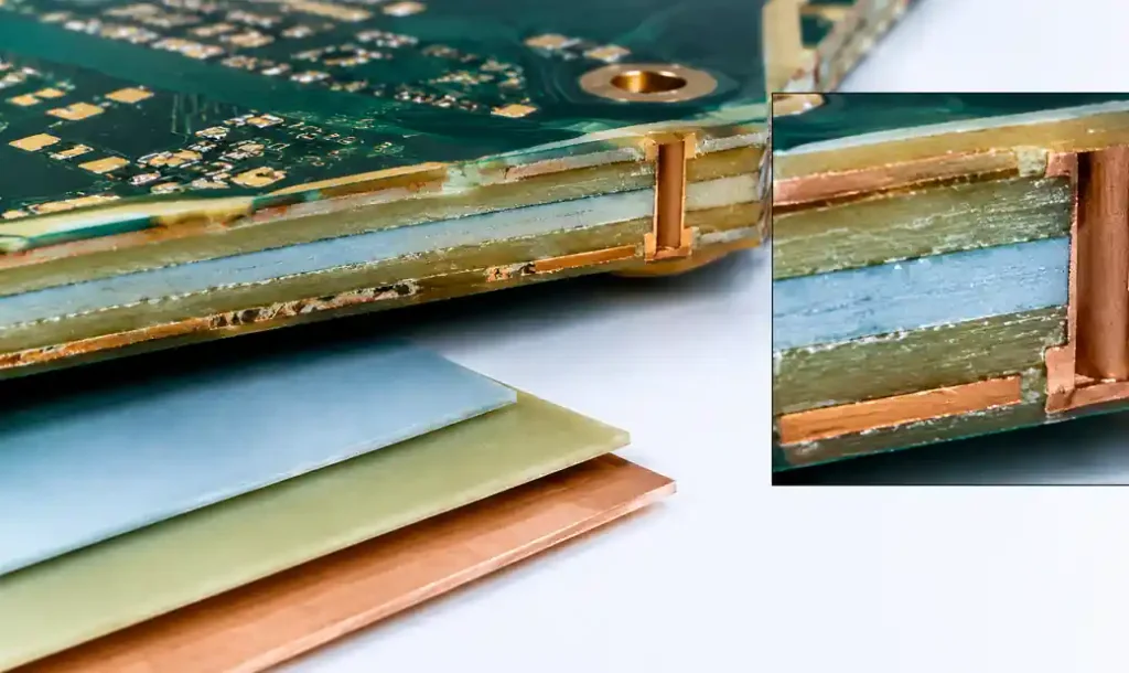
Successful Rogers/FR4 lamination requires modified press cycles with extended pressure dwell at lower temperatures (175-185°C for RO4350B versus 185-195°C for FR4-only stackups). Bond enhancer films or additional prepreg layers at interfaces improve adhesion but add cost.
| Material Interface | Bond Strength (lbs/in) | Applications | Prevention Strategy |
|---|---|---|---|
| FR4 to FR4 | 8-12 | Consumer, industrial | Standard oxide treatment |
| Rogers to FR4 | 5-7 | RF/microwave, 5G | Bond enhancer, modified cycle |
| Polyimide to FR4 | 6-9 | Rigid flex PCB, aerospace | Adhesive layers, staged lamination |
| Aluminum core to FR4 | 7-10 | LED, power electronics | Dielectric bonding film |
Quality Testing and Validation
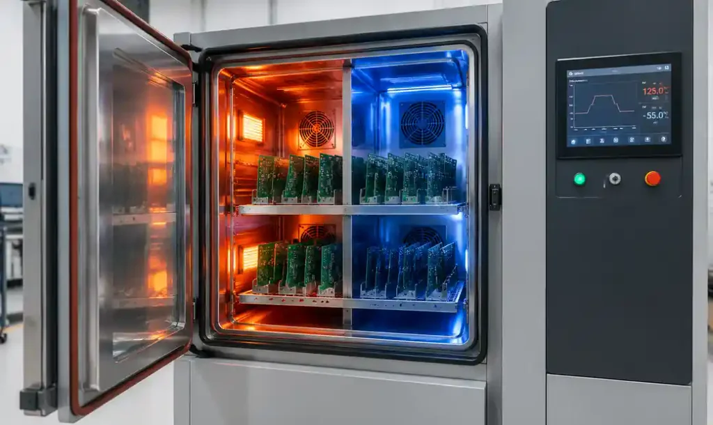
Thermal shock testing per IPC-TM-650 Method 2.6.7.1 validates delamination resistance by subjecting boards to -55°C to +125°C rapid temperature changes for 10-100 cycles. This accelerated stress reveals latent lamination defects that may not appear during standard testing but cause field failures.
Peel strength testing measures copper-to-laminate bond integrity, with IPC-6012 Class 3 requiring minimum 6 pounds per inch after thermal stress. Regular peel strength monitoring catches process degradation before customer impact. Boards showing less than 7 lbs/in have high delamination risk.
Automotive PCBs for under-hood applications face -40°C to +150°C operating range and 150-200 thermal cycles annually. These require high-Tg materials (Tg >170°C), heavy copper (2-3 oz), and controlled Z-axis CTE to survive 15-year lifespans. Medical implantable device PCBs must include C-SAM inspection data for all production lots per ISO 13485 medical device standards.
FAQ
What causes white spots or “measling” in PCB laminates?
Measling appears as white spots indicating localized delamination between glass fibers and resin matrix. This occurs when moisture absorbed in the glass-resin interface vaporizes during assembly thermal exposure, creating micro-voids. Prevention requires proper material baking (125°C for 4-6 hours) before assembly and high-Tg laminates with improved moisture resistance for multiple reflow cycles.
How does lead-free assembly increase delamination risk?
Lead-free solder requires peak reflow temperatures of 260°C versus 240°C for tin-lead, increasing thermal stress 15-20% and doubling moisture vapor pressure. PCBs for lead-free assembly require high-Tg materials (Tg 170-180°C minimum), moisture bake before assembly, and potentially thicker copper foils to handle thermal load without delamination.
Can delamination be detected before assembly?
C-SAM acoustic microscopy detects pre-existing voids and poor lamination before assembly, but delamination from thermal cycling may not appear until after temperature exposure. High-reliability manufacturers perform C-SAM inspection at both pre-assembly and post-assembly stages to ensure zero-defect delivery. Some voids remain stable through normal use but propagate under extreme conditions.
What is the difference between vacuum and standard lamination?
Vacuum lamination evacuates air from the stack before applying heat and pressure, reducing void formation by removing trapped gases. The vacuum (0.1-1 torr) also lowers moisture vaporization temperature and prevents oxidation. This adds 15-25% to cost but virtually eliminates void-related failures in aerospace and medical applications. Standard press lamination suits commercial electronics where Class 2 criteria allow minor voids.
Conclusion
Lamination voids and delamination represent critical multilayer PCB failure modes requiring systematic prevention through proper material handling, surface preparation, and press cycle optimization. Moisture contamination, surface contamination, inadequate pressure, and resin flow issues can be controlled through process discipline and real-time monitoring.
C-SAM inspection provides reliable non-destructive defect detection before assembly, while thermal shock testing validates long-term reliability. Designers reduce delamination risk through balanced copper distribution and appropriate material selection, particularly for mixed-dielectric stackups. For high-reliability applications in automotive, medical, aerospace, and telecommunications, IPC-6012 Class 3 and IATF 16949 standards ensure delamination-free performance through product lifetime.
If you need reliable multilayer PCB manufacturing with advanced lamination capabilities up to 50 layers and comprehensive C-SAM inspection, Andwin Circuits offers ISO 9001 and IATF 16949 certified production with fast turnaround in 7 days. Contact us today for custom special PCB solutions and technical specifications for your high-reliability electronic products.