
PCB Depaneling Methods: V-Cut, Routing, and Punching Comparison
When manufacturing PCBs at scale, multiple boards are fabricated on a single panel to maximize efficiency. The critical question then becomes: how do you separate them without compromising quality or introducing defects? After years of working with contract manufacturers and troubleshooting assembly-induced failures, I’ve seen firsthand how depaneling method selection directly impacts yield, component stress, and rework rates.
This guide compares the three most common mechanical depaneling methods—V-cut (V-scoring), routing, and punching—based on real production data, stress characteristics, and cost implications. Whether you’re scaling a consumer electronics product or managing tight-tolerance medical device assemblies, the method you choose affects more than just throughput.
What Is PCB Depaneling and Why Does It Matter?
Depaneling (or singulation) is the process of separating individual PCBs from a multi-unit panel after assembly. Most fabricators produce boards in arrays because it reduces material waste, speeds up SMT placement, and simplifies handling through reflow and inspection.
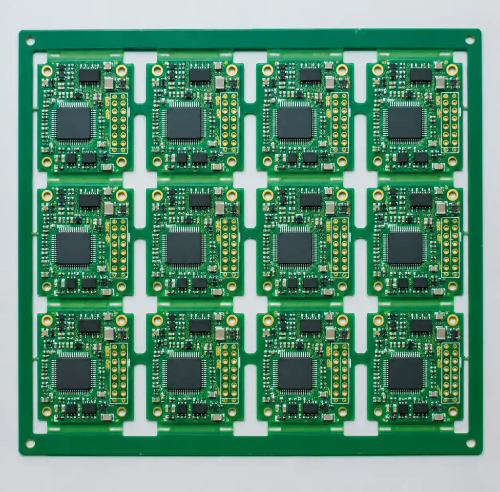
The challenge lies in the separation itself. Poor depaneling introduces microcracks in solder joints, flexes boards beyond acceptable limits, or leaves rough edges that interfere with enclosure fitment. Each method applies stress differently, and understanding those mechanics is essential for design-for-manufacturing (DFM) decisions.
According to recent industry analysis, depaneling-related defects account for 8-12% of post-assembly failures in high-mix environments, with most issues traced back to method-substrate mismatch during the design phase.
V-Cut (V-Scoring): Speed vs. Geometry Constraints
V-cut depaneling uses a circular blade to create V-shaped grooves on both sides of the panel along straight separation lines. The remaining web thickness (typically 0.3-0.5mm) allows boards to be snapped apart manually or with automated separators.
How V-Cut Works in Production
The process runs in two passes—one blade on the top surface, one on the bottom—each cutting to a controlled depth. The angle is typically 30° or 45°, leaving a thin ligament that provides panel rigidity during assembly but breaks cleanly under bending stress.
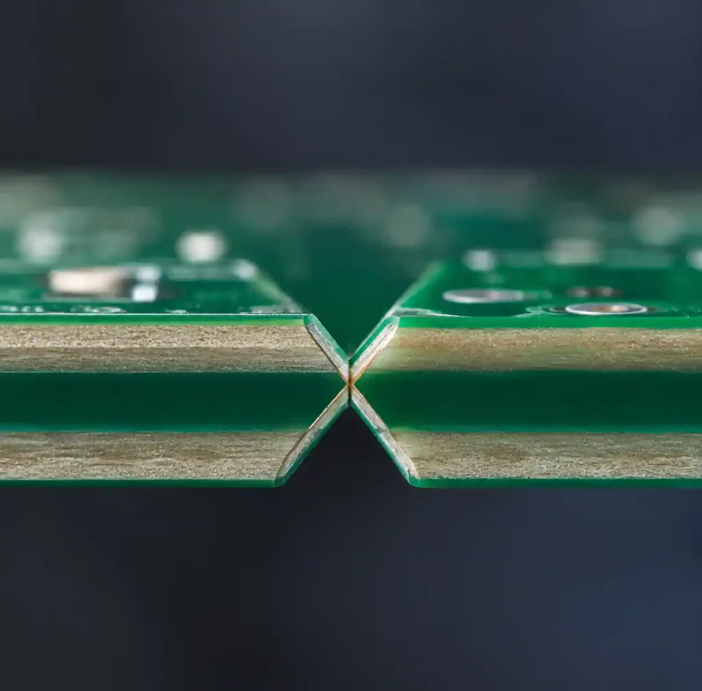
Key process parameters include blade angle, cutting depth, feed rate, and web thickness. Tighter web tolerances reduce separation force but increase the risk of premature panel breakage during handling.
Advantages of V-Cut Depaneling
Throughput and cost—V-cut is the fastest mechanical method, processing 15-20 meters per minute in automated lines. Tooling costs are minimal since the same blade handles multiple panel designs. For high-volume consumer products where board outlines are rectangular, V-cut often delivers the lowest per-unit cost.
Low equipment investment—Entry-level manual V-cut machines start under $3,000, while inline automated systems run $15,000-$30,000. This makes V-cut accessible for prototype and mid-volume production without dedicated depaneling infrastructure.
Panel stability during assembly—The continuous web keeps boards rigidly aligned through reflow, wave soldering, and AOI. This reduces warping compared to tab-routed panels, especially on larger arrays.
Limitations and Design Constraints
Straight-line geometry only—V-cut requires linear separation paths. Boards with irregular outlines, internal cutouts, or non-rectangular shapes cannot use this method. Even simple radius corners force a switch to routing.
Edge bevel remains—The V-groove leaves a beveled edge on the finished board, typically 0.3-0.8mm per side depending on blade angle and web thickness. This can interfere with edge-mounted connectors, tight enclosure fits, or stacked board assemblies. Some applications require secondary milling to square the edges.
Stress concentration at the score line—Bending the board to snap the web introduces localized stress. Components within 3-5mm of the separation line experience higher mechanical loads. In our testing, BGAs placed 2mm from a V-cut line showed a 23% increase in solder joint cracking after 500 thermal cycles compared to routing-separated controls.
Board thickness constraints—V-cut works best on 0.8-1.6mm boards. Thicker substrates (>2.0mm) require deeper grooves, which reduce the effective web strength and make clean snapping difficult. Thin flex or rigid-flex constructions (<0.6mm) lack the structural rigidity to support controlled breaking.
| V-Cut Parameter | Typical Range | Impact on Quality |
|---|---|---|
| Blade angle | 30°-45° | Deeper angles = cleaner break, wider bevel |
| Web thickness | 0.3-0.5mm | Thinner = easier separation, lower panel strength |
| Keepout zone | 3-5mm | Components closer risk stress damage |
| Panel thickness | 0.8-1.6mm | Outside range increases defect risk |
| Throughput | 15-20 m/min | Highest among mechanical methods |
CNC Routing: Flexibility and Edge Quality
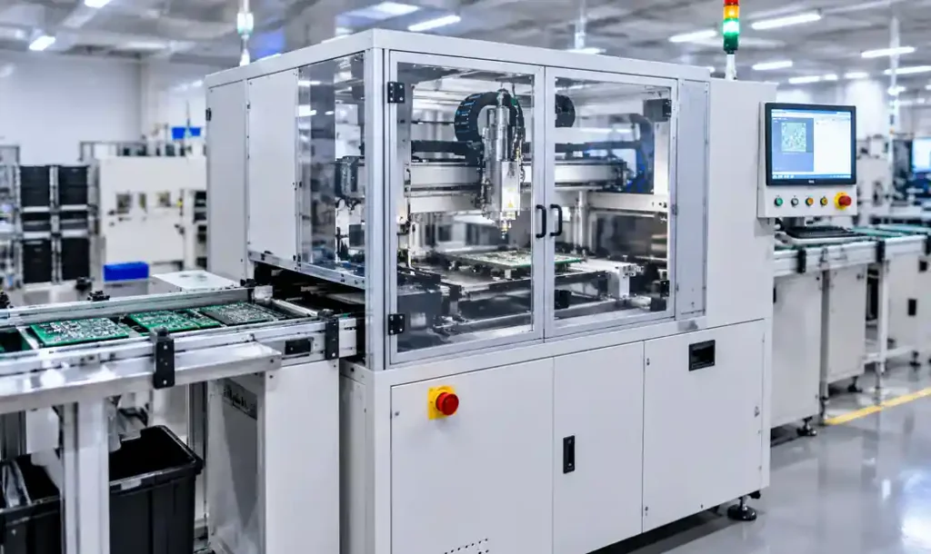
Routing uses a high-speed spindle with end mills or router bits to cut completely through the panel along programmed paths. Unlike V-cut, routing removes material rather than scoring it, producing boards with square, finished edges and supporting complex geometries.
Routing Process Details
A CNC router typically operates at 30,000-60,000 RPM with 1.0-2.0mm diameter bits. The panel is fixtured on a vacuum table or pin system, and the tool follows a programmed path that can include curves, internal cutouts, and precision slots.
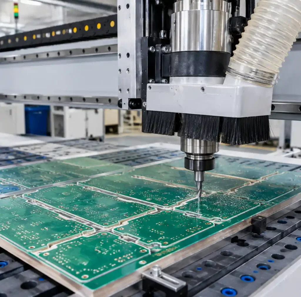
Most production routers use tab-routing, where small material tabs (0.5-1.5mm wide) connect the board to the panel frame. After routing, boards are broken or cut free from the tabs. This approach balances panel stability during assembly with clean separation afterward.
Advantages of CNC Routing
Complex board shapes—Routing handles irregular outlines, rounded corners, internal slots, and non-orthogonal edges without tooling changes. This is essential for wearables, RF modules, and boards designed to fit curved enclosures.
Square, clean edges—The routed edge is perpendicular to the board surface with minimal burr when properly programmed. Edge finish quality meets requirements for press-fit connectors, card-edge interfaces, and stacked assemblies.
Lower mechanical stress—Breaking tabs introduces localized stress, but it’s significantly less than bending an entire V-cut line. Components can be placed closer to the board edge (typically 1-2mm keepout vs. 3-5mm for V-cut).
Thickness flexibility—Routing accommodates 0.4-3.0mm boards without process changes. Rigid-flex and thick copper constructions that fail in V-cut systems route successfully with appropriate bit selection.
Disadvantages and Process Challenges
Slower throughput—Routing speed ranges from 2-8 meters per minute depending on path complexity and material. A router line processes 50-70% fewer panels per hour than V-cut for equivalent geometries.
Higher tooling and maintenance costs—End mills wear down, especially on high-Tg or ceramic-filled substrates. Bit replacement costs $3-15 per tool, and aggressive production schedules require daily changes. Dust extraction systems and spindle maintenance add to operational expenses.
Particulate generation—Routing creates fiberglass and copper dust that can contaminate assemblies if not properly extracted. Inline systems require HEPA filtration and periodic cleaning to prevent shorts and surface contamination.
Tab breakage stress—While lower than V-cut, snapping tabs still introduces mechanical stress. Poor tab design (too thin, too few, or positioned near components) can cause board flexing or solder joint damage.
| Routing Parameter | Typical Range | Impact on Quality |
|---|---|---|
| Spindle speed | 30,000-60,000 RPM | Higher speed = cleaner cut, faster bit wear |
| Bit diameter | 1.0-2.0mm | Smaller bits = tighter curves, slower cutting |
| Tab width | 0.5-1.5mm | Thinner = easier break, lower panel strength |
| Keepout zone | 1-2mm | Minimal stress near board edge |
| Throughput | 2-8 m/min | Slower than V-cut, geometry-dependent |
| Edge quality | ±0.1mm | Best mechanical method finish |
Punching (Die Cutting): High-Volume Precision
Punching uses a custom die to shear boards from a panel in a single press stroke. The die is CNC-machined to match the exact board outline, and the panel is positioned under a hydraulic or pneumatic press that forces the die through the material.
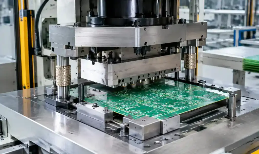
This method is common in ultra-high-volume production (>100,000 units/year) where the upfront die cost is amortized across large runs. Consumer electronics, automotive modules, and LED lighting assemblies frequently use punching for rectangular or simple-outline boards.
When Punching Makes Sense
High-volume, fixed design—Once a die is made, cycle time per board drops to 1-3 seconds. For products with stable designs and multi-year production runs, punching offers the lowest per-unit cost at scale.
Consistent edge quality—A sharp die produces repeatable, square edges with minimal variation. Unlike routing, there’s no tool wear between boards in a batch—the first and ten-thousandth board are identical.
Low operator skill requirement—Punching machines are simple to operate compared to CNC routers. Training time is minimal, and the process is less sensitive to operator technique than manual or semi-automated methods.
Punching Limitations
High tooling cost—Custom dies cost $1,500-$8,000 depending on complexity, size, and material hardness requirements. This makes punching economically unviable for prototypes or products with frequent design changes.
Limited geometry complexity—While punching handles curves better than V-cut, very tight radii (<2mm) or intricate internal features increase die complexity and cost. Extremely irregular shapes may still require routing.
Edge shear stress—Punching is a shearing process, not a cutting one. The board edge experiences high compressive and tensile forces during separation, which can microcrack the substrate or delaminate copper layers if the die is dull or misaligned.
Die wear and maintenance—Dies dull over time, especially on abrasive substrates like high-Tg FR4 or metal-core boards. A worn die produces rough edges, burrs, or incomplete cuts. Regular sharpening or replacement is required to maintain quality.
| Punching Parameter | Typical Range | Production Consideration |
|---|---|---|
| Cycle time | 1-3 sec/board | Fastest for simple geometries |
| Die cost | $1,500-$8,000 | Economical only at high volume |
| Edge tolerance | ±0.15mm | Good repeatability with sharp die |
| Keepout zone | 2-3mm | Moderate stress near edge |
| Min curve radius | ~2mm | Tighter requires complex die |
| Volume break-even | >100,000 units | Below this, routing usually cheaper |
Direct Method Comparison: When to Use Each
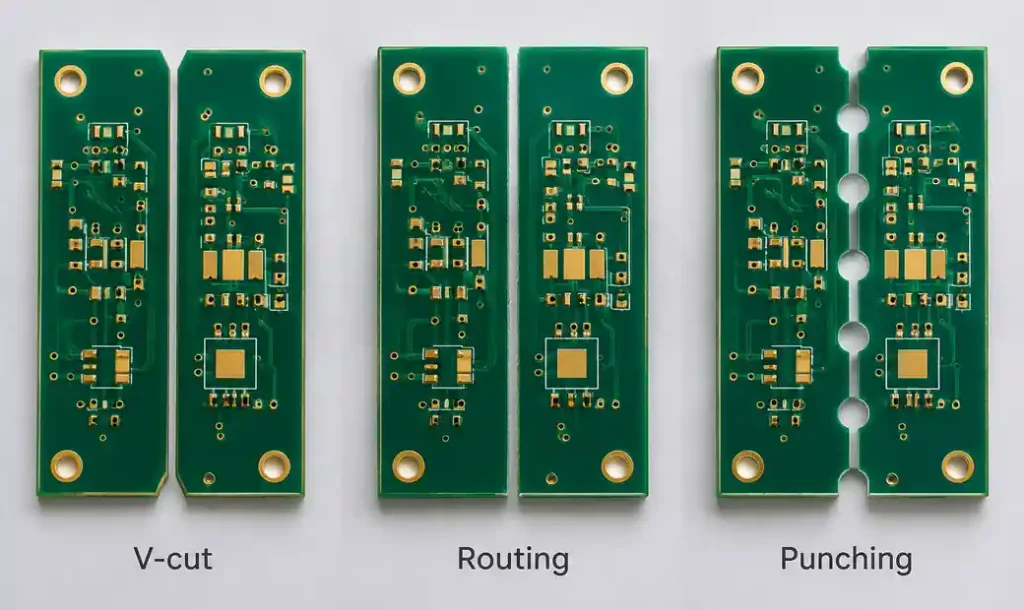
Choosing the right depaneling method depends on board geometry, production volume, component placement density, and acceptable edge finish. Here’s how they stack up in real-world production scenarios:
| Criterion | V-Cut | Routing | Punching |
|---|---|---|---|
| Board shape | Straight lines only | Any geometry | Simple to moderate curves |
| Edge finish | Beveled, rough | Square, clean | Square, repeatable |
| Throughput | 15-20 m/min | 2-8 m/min | 1-3 sec/board |
| Tooling cost | $3,000-$30,000 (machine) | $15,000-$80,000 (machine) | $1,500-$8,000 per die |
| Per-unit cost | Lowest at high volume | Moderate | Lowest above 100k units |
| Component stress | High (3-5mm keepout) | Low (1-2mm keepout) | Moderate (2-3mm keepout) |
| Substrate compatibility | 0.8-1.6mm rigid | 0.4-3.0mm rigid/flex | 0.6-2.0mm rigid |
| Setup time | <5 minutes | 15-30 minutes | 5-10 minutes |
| Design flexibility | Very low | Very high | Low (requires new die) |
Real-World Selection Examples
Consumer IoT device with 500k annual volume, rectangular board, 0.8mm FR4—V-cut delivers the fastest cycle time and lowest cost. Edge bevel is acceptable since the enclosure has clearance.
Medical wearable with irregular outline, sensitive analog circuitry, 50k annual volume—Routing provides clean edges and minimal stress near components. The shape cannot be V-cut, and volume doesn’t justify punching die cost.
Automotive LED module with fixed design, 2 million units over 3 years—Punching amortizes die cost across the production run, achieving <$0.02/board depaneling cost vs. $0.08 for routing.
Prototype run of 50 boards with complex outline—Routing is the only practical choice. V-cut won’t support the shape, and punching die cost would exceed the entire prototype budget.
DFM Considerations for Depaneling
Smart depaneling starts at the schematic phase, not after panels come back from assembly. Here’s what to lock in before layout:
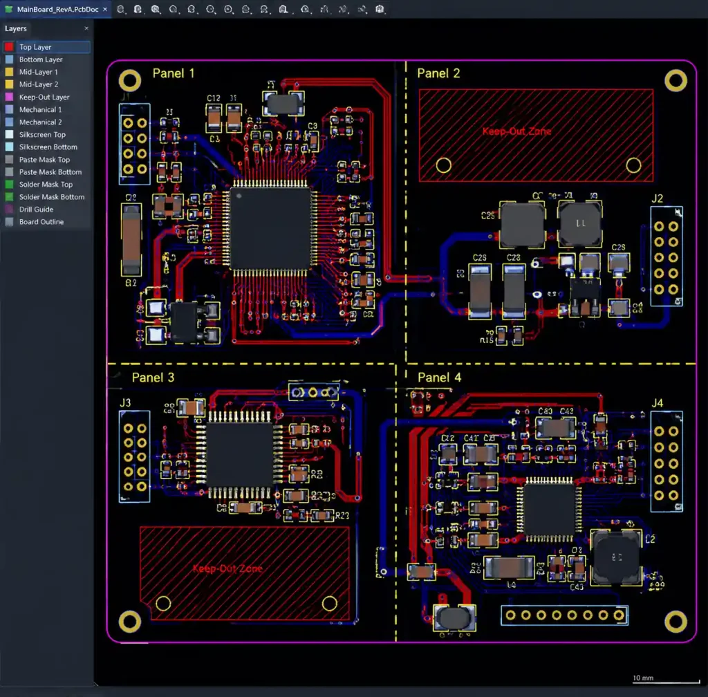
Define the method during panel design—Separation method drives keepout zones, score line placement, and tab locations. Changing methods post-layout often requires board respin.
Match component placement to stress zones—Capacitors, connectors, and BGAs are sensitive to mechanical stress. Map the stress profile of your chosen method and place critical components outside high-stress areas.
Coordinate with your CM early—Most contract manufacturers have preferred depaneling methods based on their equipment. Aligning your design with their capabilities avoids schedule delays and surprise NRE charges.
Test before scaling—Run a small batch with your chosen method and inspect solder joints under magnification after depaneling. Microcracks don’t always show up in electrical test but will cause field failures.
Common DFM Mistakes
Placing vias in V-cut score lines—The groove weakens via barrels, and bending stress can crack the plating. Keep vias at least 0.5mm clear of the score centerline.
Insufficient tab count in routed panels—Panels with fewer than 3-4 tabs per board can flex during assembly, causing tombstoning or solder bridging. More tabs add breakout time but improve yield.
Ignoring edge clearance for press-fit connectors—Punching and routing edge tolerances are typically ±0.1-0.15mm. If your connector requires <±0.05mm positioning, you may need post-depaneling machining.
Stress Testing and Quality Control
Depaneling quality isn’t binary—it’s a spectrum from pristine to catastrophically damaged. The only way to know where your boards fall is through systematic inspection and stress testing.
Visual inspection under magnification—Inspect board edges at 10-20x magnification for microcracks, delamination, or copper pullback. Even hairline substrate cracks can propagate under thermal cycling.
Solder joint cross-sectioning—Destructive analysis of joints near separation lines reveals stress-induced voiding or intermetallic layer cracking that electrical test won’t catch.
Thermal cycle testing—Subject depaneled boards to 500-1000 temperature cycles per IPC-9701 and monitor for failures. Compare results to boards separated by different methods to quantify stress delta.
Mechanical stress simulation—Finite element analysis (FEA) can model stress distribution during V-cut snapping or tab breaking. This helps optimize score line placement and tab count before committing to tooling.
At Andwin Circuits, we run cross-section analysis on first articles from every new depaneling setup to verify joint integrity before ramping production. This adds 2-3 days to NPI schedules but has caught multiple issues that would have caused field returns.
Cost Analysis: Total Cost of Ownership
Raw depaneling cost per board is only part of the equation. Defect rates, rework, and yield loss often outweigh the direct processing cost.
V-cut total cost—For a 10,000-unit run of a simple rectangular board, V-cut might cost $0.03/board in direct processing. If stress-induced defects cause 2% yield loss on a $15 assembly, that’s an additional $0.30/board in scrap cost, dwarfing the depaneling savings.
Routing total cost—Routing the same board might cost $0.12/board but reduce yield loss to 0.3%, resulting in $0.045/board scrap cost. The net result is $0.165/board total depaneling cost vs. $0.33 for V-cut.
Punching economics—If die cost is $4,000 and you’re producing 200,000 units, that’s $0.02/board in tooling amortization plus $0.02/board in processing, for $0.04/board total. But this only works if your design is stable enough to use the same die for the entire run.
Hidden costs—Don’t forget post-depaneling rework (edge deburring, flux cleaning), increased handling damage from rough edges, and engineering time spent troubleshooting stress-related failures.
Frequently Asked Questions
Can I mix depaneling methods on the same panel?
No. A panel is either V-scored, routed, or punched—you can’t use different methods on different separation lines within one panel. However, you can use routing to add internal cutouts or slots in a V-cut panel before scoring.
What’s the minimum keepout distance for V-cut near components?
Industry standard is 3mm for passives and 5mm for sensitive components like BGAs or high-pin-count connectors. Going closer requires stress testing to verify reliability.
How do I choose between manual and automated depaneling?
Manual methods (hand-snapping V-cuts, plier-breaking tabs) are acceptable for <500 units or when labor cost is very low. Above 1,000 units, automated systems reduce variability and operator fatigue-related errors.
Does board thickness affect depaneling method choice?
Yes. V-cut works best on 0.8-1.6mm boards. Routing handles 0.4-3.0mm. Punching is practical for 0.6-2.0mm. Rigid-flex and very thin boards (<0.4mm) often require laser depaneling instead of mechanical methods.
Can depaneling method affect EMI or signal integrity?
Indirectly, yes. Rough or beveled edges from V-cut can create impedance discontinuities near board-edge transmission lines. Routing produces square edges that better match controlled impedance requirements.
What’s the lead time difference between routing and punching?
Routing setup is 15-30 minutes per new panel design (program the tool path). Punching requires 2-4 weeks die fabrication lead time, but setup after that is <10 minutes.
Conclusion
Selecting the right depaneling method requires balancing throughput, cost, geometry constraints, and mechanical stress against your specific product requirements. V-cut excels in high-volume production of simple rectangular boards where speed and cost dominate. Routing provides maximum design flexibility and minimal component stress, making it the default choice for complex geometries and sensitive assemblies. Punching delivers the lowest per-unit cost at ultra-high volumes but demands stable designs and significant upfront investment.
The most expensive depaneling mistake is choosing a method late in the design cycle and then discovering it doesn’t align with your board geometry, component placement, or CM capabilities. Define your separation strategy during initial panel layout, coordinate with your manufacturing partner early, and validate through small-batch testing before committing to full production.
Depaneling is not a secondary process—it’s a critical manufacturing step that directly impacts yield, reliability, and total cost. Choose deliberately, design accordingly, and test thoroughly.