
Press-Fit Connectors on PCB: Design Guidelines and Quality Requirements
Press-fit technology accounts for over 60% of connector installations in modern telecom infrastructure and industrial control systems. According to IEC 60352-5 standards, press-fit connections demonstrate 10× higher reliability than traditional soldered joints in high-vibration environments. Eliminating wave soldering reduces thermal stress and accelerates production by 30-40%.
This guide provides hole diameter tolerances, plating thickness requirements, insertion force calculations, and IPC-6012 reliability testing specifications from telecommunications, automotive, and industrial applications.
What Are Press-Fit Connectors on PCB?
Press-fit connectors create electrical and mechanical connections by inserting compliant pins into plated through-holes (PTH) without soldering. The pin features a compliant section—typically “eye-of-the-needle” profile—that compresses elastically creating gas-tight contact with retention forces from 30N to 80N per pin.
IPC-HDBK-9798 defines press-fit as a “cold-joining” process eliminating molten solder, flux residues, and thermal cycling damage. The interference fit establishes electrical resistance below 2mΩ per contact. You should specify press-fit for backplanes, automotive PCBs, and high-density assemblies requiring rework capability.
Press-Fit vs Through-Hole Soldering: Performance Comparison
Traditional wave soldering subjects assemblies to 250-260°C causing board warpage and component stress. Press-fit operates at room temperature, reducing process time from 45-60 seconds per board to 2-5 seconds per connector.
The compliant pin maintains constant contact force across -55°C to +150°C temperature cycling. Solder joints exhibit creep and intermetallic growth degrading electrical performance. Press-fit maintains sub-2mΩ resistance for 25+ years in telecom PCB equipment.
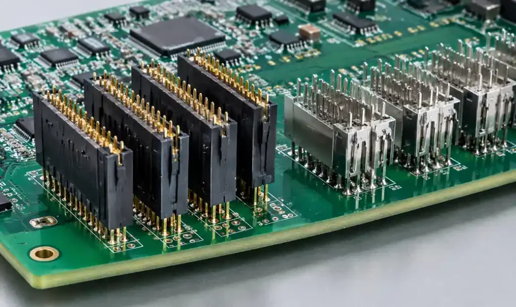
You can extract press-fit pins without damaging plated holes, allowing field replacement. Desoldering requires hot air risking pad lifting. For 200-400 pin backplanes, press-fit reduces assembly defects from 3-5% to below 0.5%.
| Parameter | Press-Fit | Wave Soldering | Selective Soldering |
|---|---|---|---|
| Process Temperature | Room temperature (20-25°C) | 250-260°C | 280-300°C peak |
| Thermal Stress | None | High | Medium |
| Insertion Force | 30-80N per pin | N/A | N/A |
| Contact Resistance | <2mΩ | <5mΩ | <5mΩ |
| Rework | Pin extraction (non-destructive) | Desolder + cleanup | Desolder + cleanup |
| Cycle Time | 2-5 sec per connector | 45-60 sec per board | 15-30 sec per connector |
| Reliability (FIT) | <50 | 100-200 | 80-150 |
PTH Diameter Tolerance and Hole Size Requirements
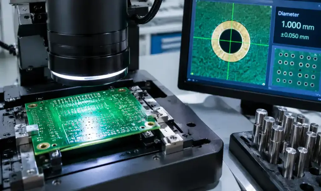
Finished hole diameter (FHD) determines insertion force and connection reliability. IPC-HDBK-9798 requires FHD tolerance of ±0.05mm for press-fit applications, tighter than standard ±0.075mm PTH tolerance. A 1.00mm compliant section requires 0.95-0.98mm FHD creating 0.02-0.05mm interference.
Measure diameter at board entry, exit, and mid-barrel because plating variations cause hour-glass profiles. For 1.6mm boards, measure at 0.8mm depth. Automated optical inspection checks every hole, rejecting boards outside ±0.025mm specification.
Drill bit wear causes 0.01-0.02mm diameter increase over 3,000-5,000 holes. Monitor diameter every 500 holes, replacing bits approaching tolerance limits. Laser drilling provides superior consistency for holes below 0.6mm.
Maintain aspect ratio below 8:1 (board thickness to diameter). A 2.0mm board requires minimum 0.25mm drill diameter. Higher ratios cause drill wander and non-uniform plating.
Plating Thickness and Surface Finish Requirements
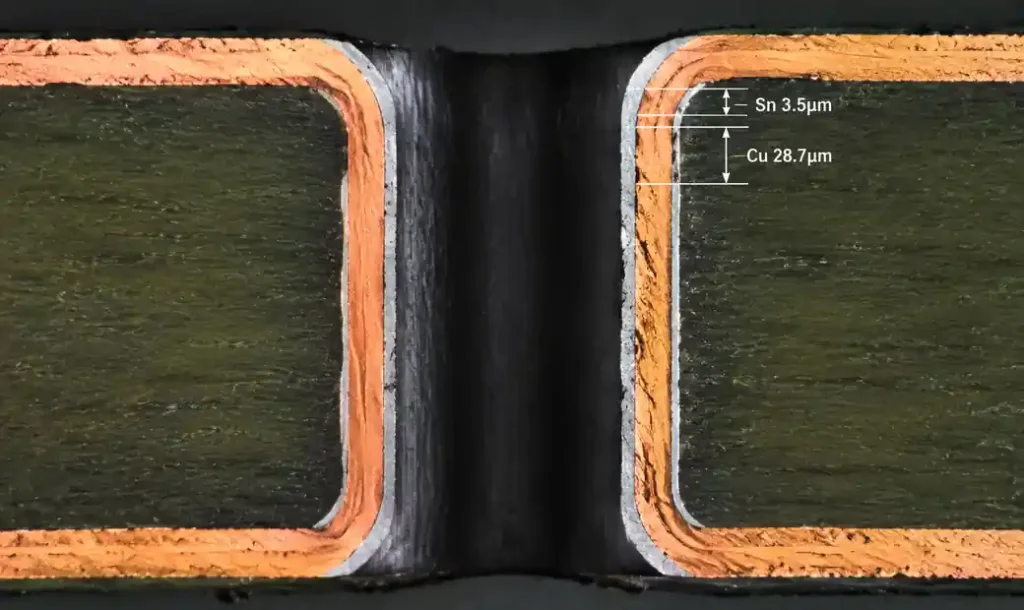
Copper plating thickness must meet 25µm minimum per IPC-6012 Class 3 for press-fit applications. Specify 30-35µm target providing margin above minimum. Measure at hole entry, mid-barrel, and exit verifying uniformity within ±20%.
Apply 5-10µm tin plating creating ductile interface conforming to pin geometry. Tin must be matte finish (1-3µm grain) rather than bright finish which becomes brittle. ENIG finish offers superior corrosion resistance for long-term storage.
Plating uniformity around barrel circumference is critical. Uneven plating creates high and low spots causing inconsistent insertion force. Specify less than 15% thickness variation. Avoid OSP or bare copper finishes which oxidize rapidly, increasing contact resistance.
Insertion Force Calculation and Control
Insertion force depends on interference fit, plating hardness, pin geometry, and board thickness. The formula: F = π × D × L × µ × P where D is hole diameter, L is thickness, µ is friction coefficient (0.15-0.25), and P is contact pressure (20-40 MPa).
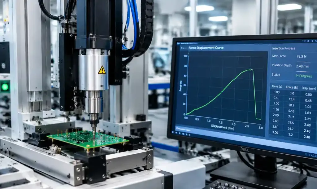
For 1.00mm pin with 0.03mm interference in 1.6mm board: F ≈ 29-45N. Specify insertion force limits: minimum 30N confirming adequate interference, maximum 80N preventing hole damage.
Press-fit equipment must control force and displacement. Pneumatic presses provide force regulation using pressure feedback. Servo-electric presses offer displacement control stopping at precise depth. Monitor force-displacement curves detecting anomalies.
Insertion depth tolerance is ±0.2mm for through-hole pins. Incomplete insertion reduces contact area. Over-insertion can fracture pins or crack boards. Use hard-stop fixtures ensuring repeatable control.
Reliability Testing Per IEC 60352-5 and Thermal Cycling
IEC 60352-5 establishes reliability requirements for solderless press-in connections. Contact resistance must remain below 2mΩ at 100mA test current, measured using four-wire Kelvin method eliminating lead resistance. Perform initial resistance measurement, then after thermal cycling, vibration, and mechanical stress testing.
Thermal cycling from -55°C to +150°C for 1,000 cycles per IPC-9701 qualification validates long-term stability. Press-fit connections exhibit minimal resistance change (<0.5mΩ increase) because elastic interference maintains contact pressure across CTE mismatches. Solder joints show 2-5mΩ degradation from intermetallic growth and microcracking.
Vibration testing per IPC-HDBK-9798 requires 10-50 Hz sinusoidal vibration at 5g acceleration for 12 hours per axis. Monitor contact resistance during vibration detecting intermittent opens. Press-fit connections outperform solder by eliminating fatigue crack propagation at the joint interface.

Retention force testing measures pin extraction force after environmental exposure. Pull each pin with tensile tester at 5mm/min rate. Minimum retention force is 50% of insertion force, typically 15-40N per pin. Retention below minimum indicates plating deformation or hole damage requiring root cause analysis.
| Test Parameter | Test Method | Acceptance Criteria | Standard |
|---|---|---|---|
| Contact Resistance (initial) | 4-wire Kelvin @ 100mA | <2mΩ | IEC 60352-5 |
| Thermal Cycling | -55°C to +150°C, 1,000 cycles | ΔR <0.5mΩ | IPC-9701 |
| Vibration | 10-50 Hz, 5g, 12h per axis | No intermittent opens | IPC-HDBK-9798 |
| Retention Force | Pull test @ 5mm/min | >50% insertion force | IEC 60352-5 |
| Humidity | 85°C/85%RH, 1,000h | ΔR <1mΩ | IPC-TM-650 |
Design Guidelines for PCB Layouts with Press-Fit Connectors
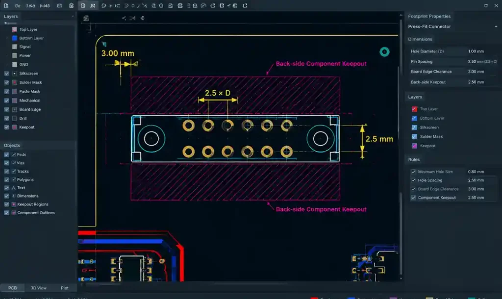
Position press-fit holes minimum 3mm from board edges preventing edge cracking. Hole-to-hole spacing must exceed 2.5× hole diameter or 2.0mm minimum. Closer spacing risks plating cracks or hole distortion.
Locate press-fit zones away from mounting holes and cutouts where board flex concentrates. Provide 5mm clearance zones around press-fit areas free from surface mount components interfering with insertion tooling.
Maintain 3mm clearance on opposite board surfaces aligned with press-fit holes. Components directly opposite experience impact stress during insertion potentially cracking solder joints. Use teardrop pad designs distributing stress and increasing adhesion by 30-40%.
Implement symmetrical stackups for boards using press-fit. Unbalanced copper causes warpage affecting hole perpendicularity and insertion force variability.
Cost Considerations and Production Efficiency
Press-fit pins cost $0.02-$0.08 per pin versus $0.01-$0.03 for standard pins, adding $5-$20 material cost for 100-200 pin connectors. PCB fabrication cost increases $10-$30 per board due to tighter tolerances. However, eliminating wave soldering saves $30,000-$80,000 in capital equipment per line.
Assembly labor reduces significantly. Wave soldering requires 60-90 seconds per board plus operator time. Automated press-fit completes 100-200 pins in 10-20 seconds. At 500+ boards daily, labor savings exceed material costs within 12-18 months.
Defect reduction provides additional benefits. Press-fit eliminates cold solder joints and bridging. Defect rates drop from 3-5% to below 0.5%. Each avoided rework saves 5-10 minutes labor plus materials.
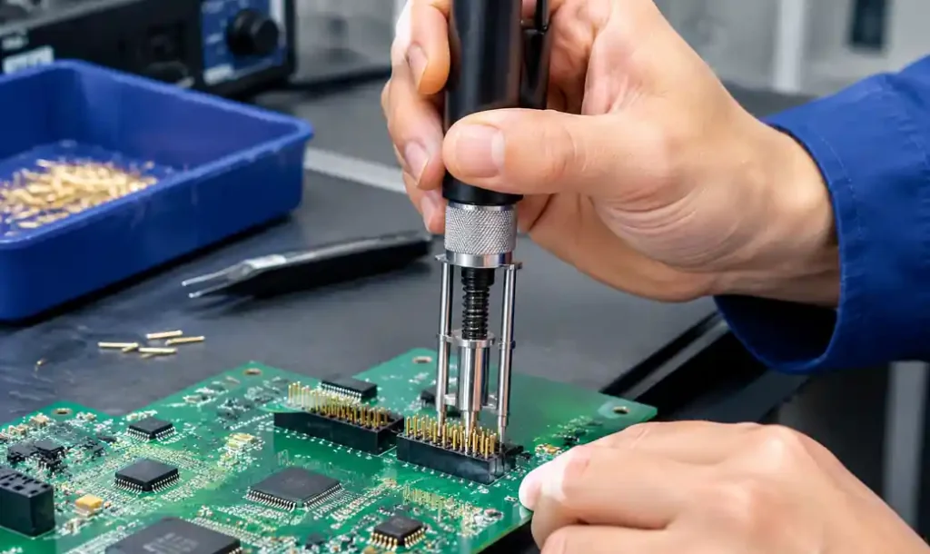
Field serviceability extends product value. Technicians replace press-fit connectors using portable extraction tools without specialized soldering equipment, reducing downtime from days to hours.
Rework and Field Service Procedures
Extraction tools apply controlled tensile force removing pins without barrel damage. Manual extractors use lever mechanisms generating 100-150N force. Pneumatic extractors provide precise control stopping at preset limits.
Inspect extracted holes using optical microscopy at 20-50× magnification detecting plating damage. Holes showing cracks or diameter growth exceeding 0.05mm should not accept new pins.
Measure insertion force for replacement pins comparing to original values. Forces below 70% of specification indicate hole damage requiring repair. Document insertion/extraction cycles for each location. IEC 60352-5 requires connections withstand minimum 3 cycles maintaining specifications.
Frequently Asked Questions
What is the maximum board thickness for press-fit connectors?
Standard compliant pins support board thickness up to 3.2mm. For thicker boards (3.2-5.0mm), specify long-barrel press-fit pins with extended compliant sections. Boards exceeding 5.0mm may require multiple-piece stackable connectors or transition to soldered connections.
Can you mix press-fit and soldered connections on the same board?
Yes. Design press-fit zones with controlled plating separate from SMT assembly areas. Mask press-fit holes during wave or selective soldering preventing solder wicking. Apply press-fit connectors after soldering to avoid thermal exposure.
How does humidity affect press-fit connection reliability?
Tin-plated contacts resist corrosion in industrial environments. Specify conformal coating or selective potting for harsh environments exceeding 85°C/85%RH. ENIG finish provides superior corrosion resistance for long-term storage or tropical climates.
What insertion speed provides optimal results?
Control insertion velocity between 10-25 mm/sec. Excessive speed (>50 mm/sec) generates heat from friction potentially softening tin plating and increasing insertion force. Slow insertion (<5 mm/sec) extends cycle time without benefit. Pneumatic presses naturally achieve optimal speed through pressure regulation.
Are press-fit connectors suitable for automotive applications?
Yes. Automotive ECUs and infotainment systems extensively use press-fit. Specify per IPC-HDBK-9798 automotive requirements including AEC-Q200 qualification and extended cycling from -40°C to +125°C. Vibration resistance and rework capability make press-fit ideal for automotive electronics.
Conclusion
Press-fit connector technology delivers superior reliability and manufacturing efficiency for high-density PCB assemblies in telecommunications, automotive, and industrial applications. Controlling finished hole diameter within ±0.05mm tolerance, maintaining 25-35µm copper plating thickness, and specifying appropriate tin finish creates connections that outperform wave soldering by 10× in long-term reliability testing. The elimination of thermal stress, combined with room-temperature assembly and rework capability, reduces defect rates below 0.5% while accelerating production throughput by 30-40% compared to traditional soldering processes. Implementing IEC 60352-5 qualification testing and IPC-HDBK-9798 design guidelines ensures 25+ year service life in demanding environments.
If you need PCB manufacturing with tight hole tolerances and precise plating control for press-fit connector assemblies, Andwin Circuits provides ISO 9001 and IATF 16949 certified production with capability up to 50 layers. Our advanced drilling and plating processes achieve ±0.025mm hole accuracy and uniform 30-35µm copper thickness. Fast delivery in 7 days for prototypes ensures your product development stays on schedule.
Contact us today for custom PCB solutions supporting press-fit technology with IPC Class 3 quality standards.