
Selective Soldering: When to Use It Instead of Wave Soldering
Selective soldering is the right choice when your PCB assembly combines surface mount and through-hole components, when thermal sensitivity prohibits wave soldering’s full-board exposure, or when production volumes don’t justify wave equipment but demand better quality than hand soldering. The decision hinges on component density, heat tolerance, joint count, and whether your design has pre-reflowed SMT devices that wave soldering would damage.
If you’re assembling mixed-technology boards where 70-80% of components are SMT and only connectors, high-current terminals, or mechanical anchors remain through-hole, selective soldering delivers consistent joint quality without the thermal stress, adhesive process, and SMT tombstoning risks that wave soldering creates on modern boards.
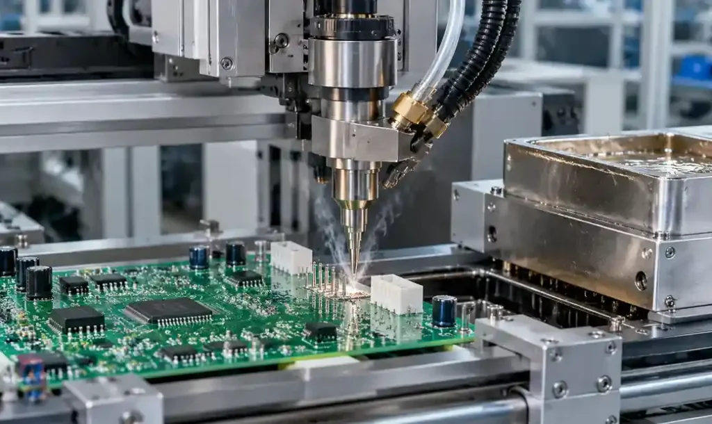
What is Selective Soldering?
Selective soldering applies a localized solder wave or solder pot to specific through-hole joints programmed into the machine’s path, leaving the rest of the board unexposed. This targeted approach solders only designated areas while protecting temperature-sensitive components, pre-reflowed SMT devices, and complex board geometries from unnecessary heat exposure.
The process uses three sequential stations: fluxing, preheating, and soldering. Flux application can be spray, drop-jet, or microjet, depending on joint density and board layout. Preheat brings the target area to 80-120°C, reducing thermal shock when the solder nozzle contacts the joint. The soldering station uses a single-point nozzle, mini-wave, or dual-wave configuration to create the solder joint at 260-280°C for 1-3 seconds per location.
You can use selective soldering for PCB assembly when boards contain mixed technology (SMT + THT), when sensitive components prohibit full wave exposure, when production volumes range from 500-5,000 units monthly, or when design changes occur frequently and dedicated wave pallets become cost-prohibitive.
Wave Soldering Process and Limitations
Wave soldering passes the entire underside of a populated PCB over a continuous pumped wave of molten solder at 250-260°C. The board travels through fluxing, preheating (100-130°C ramp over 60-90 seconds), and dual-wave soldering zones. The first turbulent wave fills vias and through-holes; the second smooth wave levels the joints and removes bridging.
The process excels at high-volume through-hole assembly, processing 40-60 boards per minute with minimal operator intervention. Wave soldering delivers the lowest cost per joint for pure THT designs or legacy products where all components tolerate 250°C+ exposure.
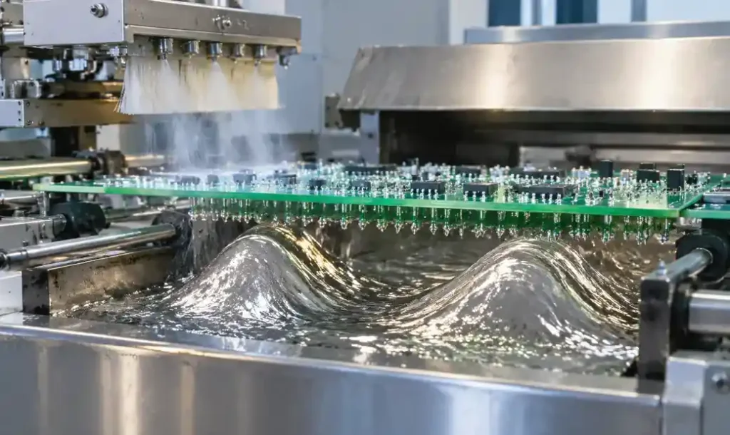
Wave soldering limitations become critical on mixed-technology boards. Pre-reflowed SMT components—already soldered during reflow—face a second thermal cycle that risks package delamination, solder joint cracking, or moisture sensitivity level (MSL) violations. Components rated for single reflow (260°C peak) may fail when wave soldering adds a second 250°C exposure. Bottom-side SMT devices require adhesive dots to prevent dropping during wave, and this adhesive process adds cost, cycle time, and potential contamination under components like QFNs and BGAs.
Mixed-Technology Wave Soldering Challenges
| Challenge | Impact | Mitigation Cost |
|---|---|---|
| SMT thermal stress | 8-15% rework rate from cracked solder joints, delamination | Adhesive application, inspection |
| Tombstoning on passives | 5-10% defect rate on 0603/0402 components | Adhesive, glue cure oven |
| Shadow effect | Insufficient solder penetration behind tall components | Custom pallet design, angle adjustment |
| Pallet tooling | $800-2,000 per design, 2-3 week lead time | Design validation, iteration |
The shadow effect occurs when tall through-hole components block the solder wave from reaching adjacent lower joints, creating voids or insufficient solder fill. Correcting this requires custom pallets with cutouts or angled board orientation, adding engineering time and tooling cost to every design revision.
When to Choose Selective Over Wave Soldering
Choose selective soldering when your board design and production volume meet these conditions: mixed SMT/THT assembly where reflowed components outnumber through-hole joints, production volumes between 500-10,000 units monthly, frequent design changes that make wave pallets impractical, or when IPC-A-610 Class 3 reliability is required for medical or automotive applications.
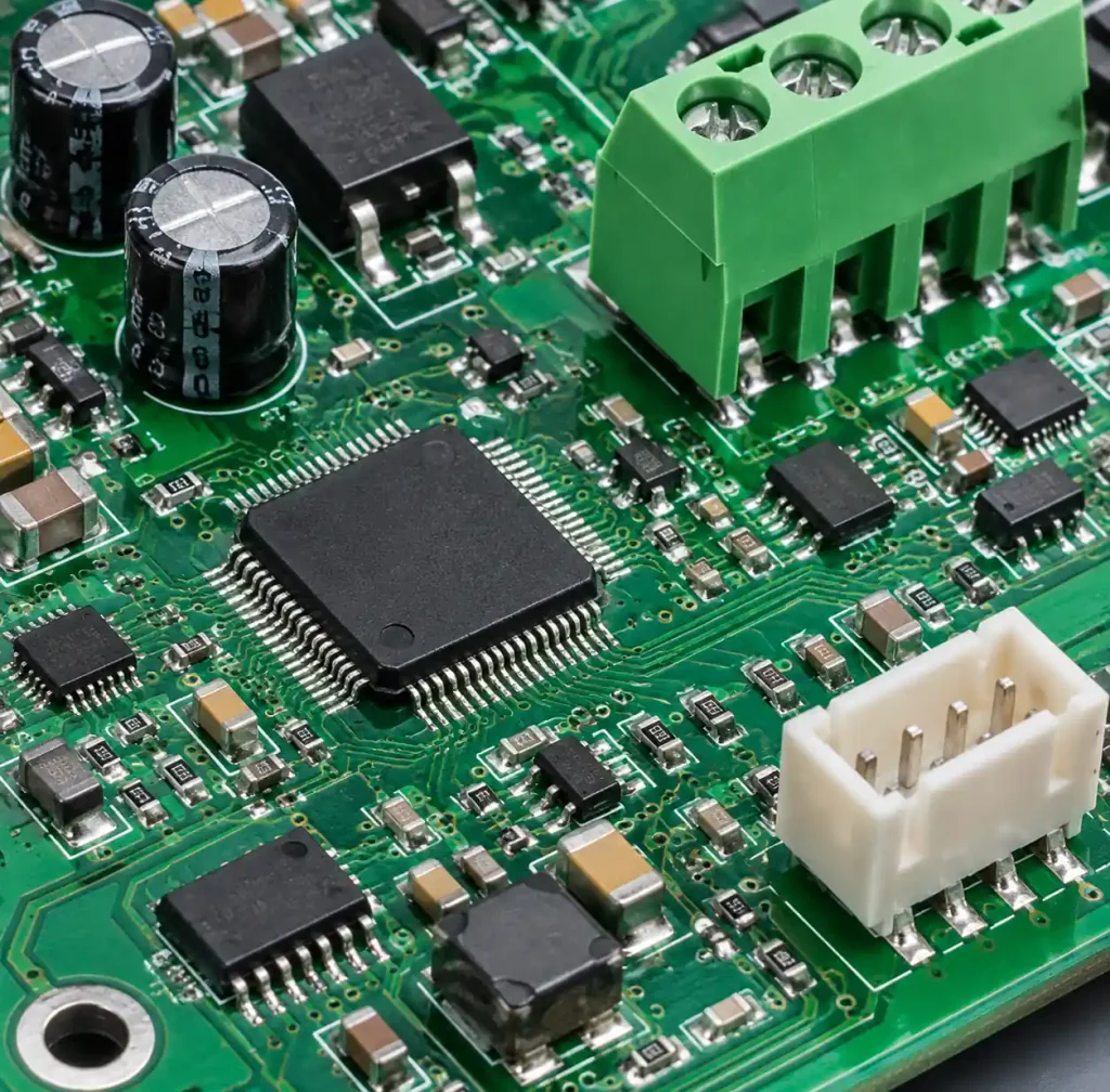
Design Scenarios Favoring Selective Soldering
Scenario 1: Dense SMT with through-hole connectors. Industrial control boards with 200+ SMT components and 5-10 THT connectors or power terminals. Wave soldering would require adhesive for all bottom SMT devices and risk thermal damage to reflowed ICs. Selective soldering targets only the connector joints, leaving SMT untouched. Joint count under 50 keeps cycle time acceptable at 8-12 boards per hour.
Scenario 2: Thermal-sensitive components. Boards containing temperature-sensitive sensors, MEMS devices, or components with MSL 3-4 ratings that cannot survive wave’s extended thermal exposure. Selective soldering’s localized heating limits thermal stress to specific zones while keeping sensitive areas under 150°C.
Scenario 3: Prototype and low-volume production. Orders of 100-2,000 units where wave soldering’s pallet tooling cost ($800-2,000) and lead time (2-3 weeks) cannot be justified. Selective soldering requires only program creation (2-4 hours) with no hard tooling, making it cost-effective for quick-turn and NPI builds.
Scenario 4: High-reliability joints. Applications requiring IPC-A-610 Class 3 acceptance criteria where selective soldering’s controlled process parameters, short dwell time (1-3 seconds), and programmable path eliminate defects common in wave soldering such as bridging, shadowing, and insufficient hole fill.
Selective Soldering Equipment and Process Control
Modern selective soldering systems integrate closed-loop monitoring with real-time adjustment of flux volume, preheat temperature, nozzle depth, and contact time. Closed-loop nitrogen control maintains oxygen below 500 ppm, reducing dross and improving wetting.
Selective Soldering Station Configuration
| Parameter | Typical Range | Impact on Quality |
|---|---|---|
| Nozzle diameter | 2-12mm | Joint accessibility, cycle time |
| Solder pot temperature | 260-280°C | Wetting speed, thermal stress |
| Dwell time | 1-3 seconds | Hole fill, intermetallic formation |
| Nitrogen flow | 20-40 L/min | Dross reduction, joint appearance |
| Preheat delta-T | 80-120°C | Thermal shock prevention |
The nozzle selection determines which joints can be reached. Standard round nozzles (4-8mm diameter) handle most connector pins and terminals. Mini-wave nozzles (10-15mm wide) solder multiple pins simultaneously on connectors with 2.54mm pitch or greater. Dual-nozzle systems switch between nozzles automatically based on joint geometry.
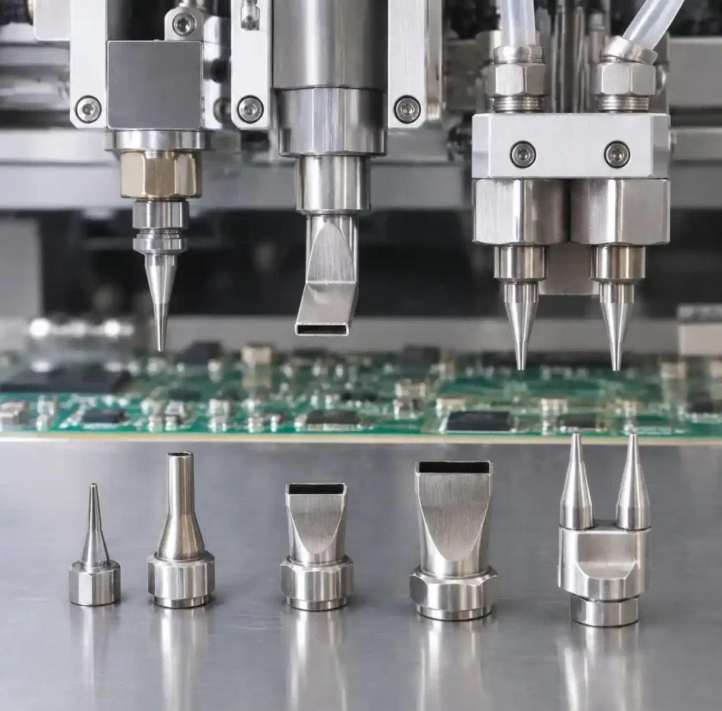
Flux application accuracy directly affects joint quality. Drop-jet fluxing deposits 0.2-0.5µL per drop with ±0.1mm placement accuracy. This precision reduces flux residue compared to wave soldering’s spray fluxing. Residue matters for no-clean flux and when conformal coating follows assembly.
Process Window and Defect Prevention
Selective soldering’s narrow process window demands careful parameter optimization. Insufficient dwell time (under 1.5 seconds) causes cold joints. Excessive dwell time (over 3.5 seconds) creates intermetallic issues and increases PCB thermal stress. Nozzle immersion depth must be 0.5-1.0mm above the board surface; deeper immersion risks bridging.
Solder bridging occurs when nozzle diameter exceeds pad clearance by more than 0.5mm. Preventing bridges requires nozzle selection based on pad pitch. Insufficient hole fill happens when preheat is inadequate (delta-T under 80°C) or when nozzle withdrawal speed exceeds 5mm/second.
Cost Analysis: Selective vs Wave Soldering
Wave soldering machines range from $80,000-250,000. Selective soldering systems cost $120,000-350,000 due to robotic motion control and vision alignment. Operating costs include solder, nitrogen, flux, maintenance, and labor.
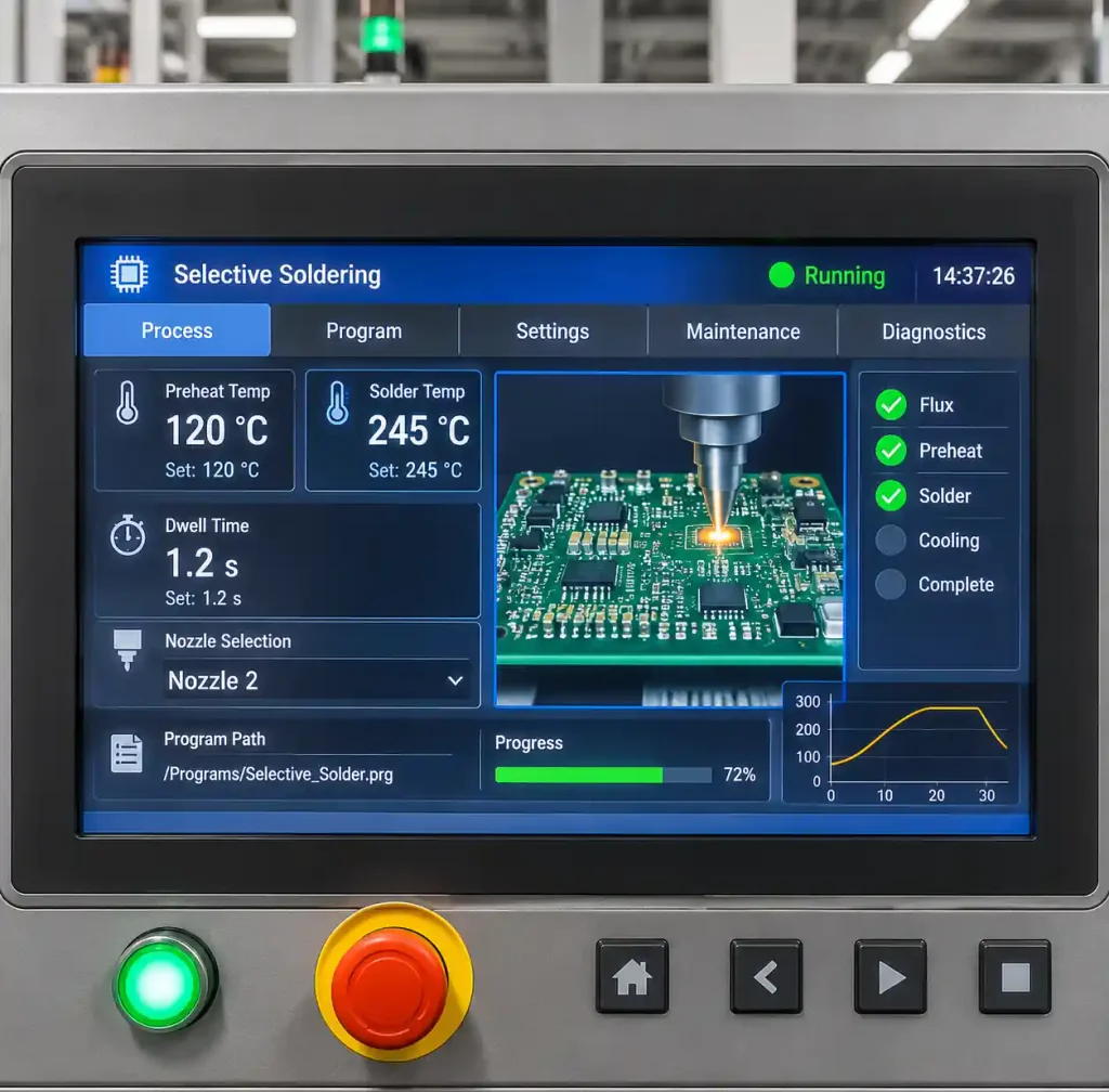
Cost Per Joint Comparison
Wave soldering achieves $0.002-0.005 per joint at volumes above 10,000 units monthly. Selective soldering costs $0.08-0.15 per joint due to slower cycle time (5-15 boards/hour vs 40-60 for wave). The crossover point occurs around 2,000-5,000 units monthly depending on joint count.
For mixed-technology boards, calculate total cost including adhesive, rework rate, and pallet tooling. Wave soldering’s low per-joint cost is offset by 8-15% rework on SMT devices and adhesive cost ($0.20-0.40 per board). Selective soldering eliminates adhesive and reduces rework to 2-5%.
When wave wins: pure THT boards with 50+ joints, volumes exceeding 10,000 units monthly, stable designs, and components rated for dual thermal cycles.
When selective wins: mixed-technology boards with under 50 THT joints, volumes 500-5,000 monthly, frequent design changes, or thermal-sensitive components.
Design Guidelines for Selective Soldering
PCB layout for selective soldering requires attention to nozzle accessibility, thermal mass distribution, and component proximity. Through-hole pads need 0.5mm minimum clearance from adjacent components for nozzle approach. Components taller than 25mm within 5mm of target joints create shadowing that blocks nozzle access.
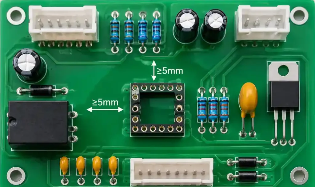
Layout Rules for Nozzle Access
Through-hole component placement must account for nozzle approach direction. Standard practice places THT components in rows with consistent orientation, allowing single-pass soldering. Scattered through-hole locations increase cycle time as the robot repositions between joints.
Pad geometry affects joint quality. Through-hole pads should be 0.3-0.5mm larger than hole diameter on both layers. Annular ring width of 0.2mm minimum ensures mechanical strength. Thermal reliefs on inner layers prevent excessive heat sinking.
Ground planes near selective soldering joints increase thermal mass, requiring longer preheat. Best practice limits continuous copper under THT pads to 100mm² or uses thermal reliefs with 0.5mm spoke width.
Comparison Table: Selective vs Wave Soldering Decision Matrix
| Criterion | Selective Soldering | Wave Soldering |
|---|---|---|
| Best application | Mixed SMT/THT, <50 THT joints | Pure THT or legacy designs |
| Production volume | 500-10,000 units/month | >10,000 units/month |
| Cycle time | 5-15 boards/hour | 40-60 boards/hour |
| Cost per joint | $0.08-0.15 | $0.002-0.005 |
| Tooling cost | $0 (program only) | $800-2,000 per design |
| SMT thermal stress | None (localized heating) | High (full-board exposure) |
| Setup time | 2-4 hours (programming) | 1-2 days (pallet + parameters) |
| Design flexibility | High (easy reprogramming) | Low (pallet redesign required) |
| Defect rate | 2-5% (bridging, insufficient fill) | 8-15% (SMT damage, tombstoning) |
Frequently Asked Questions
Can selective soldering handle fine-pitch connectors under 1.27mm pitch?
Yes, selective soldering with mini-wave nozzles reliably solders connectors down to 1.0mm pitch when pad design follows IPC-7351 guidelines and nozzle width matches the connector footprint. Pitches below 1.0mm require individual pin soldering with single-point nozzles, increasing cycle time proportionally. Most HDI PCB assemblies with fine-pitch through-hole components use selective soldering to avoid wave soldering’s bridging risk.
What is the maximum board thickness for selective soldering?
Selective soldering handles PCB thickness from 0.4mm-6.0mm without modification. Boards exceeding 3.2mm thickness require extended preheat time (100-150 seconds) to bring internal layers to adequate temperature for solder wetting. Thick boards with high copper content may need custom preheat profiles and higher solder pot temperatures (275-280°C) to achieve acceptable hole fill. The limitation is thermal mass, not mechanical capability.
Does selective soldering work with lead-free alloys?
All modern selective soldering equipment supports SAC305 (Sn96.5Ag3.0Cu0.5) and other lead-free alloys that comply with RoHS and REACH regulations. Lead-free soldering requires higher pot temperature (270-280°C vs 250-260°C for Sn63Pb37), tighter nitrogen atmosphere control (under 300 ppm O₂), and optimized flux chemistry. Wetting performance and joint appearance match tin-lead when process parameters are correctly tuned.
How does selective soldering affect assembly lead time?
Selective soldering adds 1-2 days to total assembly lead time compared to hand soldering, but reduces lead time by 3-5 days compared to wave soldering due to eliminated pallet design and fabrication. Programming a selective soldering process for a new board takes 2-4 hours including first-article inspection. The time investment is front-loaded in process development, making selective soldering ideal for prototype PCB assembly and quick-turn production.
Can I convert a wave soldering process to selective soldering?
Yes, conversion is straightforward when through-hole joint count is under 100 per board. The conversion eliminates adhesive application equipment, reduces flux consumption by 60-80%, and removes pallet tooling inventory. Key steps include programming joint locations, optimizing preheat profile for localized heating, and selecting appropriate nozzle sizes. Most PCBA manufacturers maintain both wave and selective capabilities to handle different product families cost-effectively.
Conclusion
Selective soldering fits the modern reality of PCB assembly where most components are surface mount and through-hole elements serve structural, power, or interface roles. The decision to use selective instead of wave soldering depends on joint count, thermal sensitivity, production volume, and total process cost including rework and tooling.
Choose selective soldering when your boards combine SMT and THT with under 50 through-hole joints, when thermal-sensitive components prohibit wave exposure, when production volumes range from 500-10,000 units monthly, or when design iterations make wave pallet tooling impractical. Wave soldering remains the cost leader for pure through-hole designs above 10,000 units monthly where all components tolerate full-board thermal exposure.
The process technology continues advancing. Latest selective soldering systems integrate AI-driven process optimization, automatic nozzle changing, and real-time X-ray joint inspection that closes the quality gap with manual soldering while maintaining selective’s automation benefits. For mixed-technology assemblies, selective soldering delivers the joint quality, flexibility, and cost structure that matches modern electronics manufacturing requirements.