
Automated Optical Inspection (AOI) in PCB Manufacturing: Principles, Benefits, and Challenges
1. Introduction
Printed Circuit Boards (PCBs) are the backbone of modern electronics, enabling the interconnection of components in devices ranging from smartphones to industrial machinery. As PCBs become more complex with higher component density and finer traces, ensuring manufacturing quality has become increasingly critical. Automated Optical Inspection (AOI) is a key technology used in PCB manufacturing to detect defects early in the production process, improving yield and reducing costs.
This article explores the principles of AOI, its applications in PCB inspection, benefits, challenges, and future trends.
2. What is AOI in PCB Inspection?
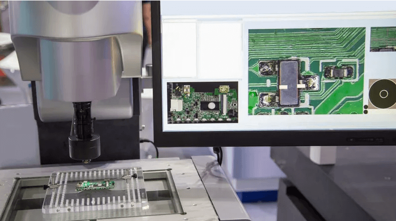
AOI is a non-contact, vision-based inspection system that uses high-resolution cameras, lighting, and image processing algorithms to detect defects in PCBs. It is typically deployed at multiple stages of PCB manufacturing, including:
- Post-Solder Paste Inspection (SPI) – Verifies solder paste deposition before component placement.
- Post-Pick and Place (Pre-Reflow) – Checks component placement accuracy before soldering.
- Post-Reflow Inspection – Examines solder joints and component alignment after reflow soldering.
- Final Inspection – Ensures the assembled PCB meets quality standards before shipment.
AOI systems compare captured images of the PCB against a reference design (CAD data or a “golden board”) to identify discrepancies such as missing components, misalignment, solder defects, and trace damage.
3. How AOI Works in PCB Inspection
3.1 Image Acquisition
AOI systems use high-resolution cameras (monochrome or color) with advanced lighting techniques (e.g., coaxial, side lighting, or strobe lighting) to capture detailed images of the PCB. Different lighting angles help reveal various defects, such as:
- Solder bridging (short circuits between pads)
- Insufficient/excessive solder
- Component misalignment or tombstoning
- Missing or wrong components
- Scratches or copper trace defects
3.2 Image Processing & Defect Detection
Once images are captured, AOI software processes them using:
- Template Matching – Compares the PCB against a known good reference.
- Pattern Recognition – Identifies deviations in component placement.
- Algorithm-Based Analysis – Detects anomalies in solder joints, traces, and component polarity.
Machine learning (ML) and artificial intelligence (AI) are increasingly used to improve defect classification and reduce false positives.
3.3 Reporting & Feedback
Detected defects are logged, and the system can:
- Flag defective boards for rework.
- Provide real-time feedback to adjust manufacturing parameters (e.g., solder paste application).
- Generate statistical process control (SPC) data for continuous improvement.
4. Benefits of AOI in PCB Manufacturing
4.1 Improved Quality Control
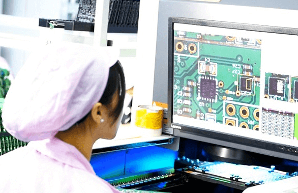
AOI detects defects that manual inspection might miss, such as micro-cracks, tiny solder bridges, or incorrect component values. This reduces the risk of faulty PCBs reaching customers.
4.2 Faster Inspection Speed
Manual inspection is slow and prone to human error, whereas AOI can scan hundreds of PCBs per hour with consistent accuracy.
4.3 Cost Reduction
Early defect detection prevents costly rework or recalls. By catching issues before final assembly, manufacturers save on scrap and warranty claims.
4.4 Traceability & Data Analytics
AOI systems store inspection data, enabling root cause analysis and process optimization. Manufacturers can track defect trends and improve yields over time.
4.5 Compatibility with Industry 4.0
AOI integrates with smart factory systems, supporting real-time monitoring and automated process adjustments.
5. Challenges and Limitations of AOI
Despite its advantages, AOI has some limitations:
5.1 False Positives/Negatives
- Overly sensitive settings may flag acceptable variations as defects (false positives).
- Some defects (e.g., hidden solder joints under components) may go undetected (false negatives).
5.2 High Initial Investment
Advanced AOI systems require significant capital expenditure, which may be a barrier for small manufacturers.
5.3 Programming Complexity
Setting up AOI for new PCB designs requires precise calibration and algorithm tuning, which can be time-consuming.
5.4 Limited Coverage for Certain Defects
AOI may struggle with:
- Internal layer defects (requires X-ray inspection, AXI).
- Component functionality testing (requires in-circuit testing, ICT, or flying probe testing).
6. AOI vs. Other PCB Inspection Methods
| Inspection Method | Technology | Strengths | Limitations |
|---|---|---|---|
| AOI | Optical imaging | Fast, non-contact, detects surface defects | Limited to visible defects, false positives |
| AXI (Automated X-ray Inspection) | X-ray imaging | Detects hidden solder joints (e.g., BGA) | Expensive, slower than AOI |
| ICT (In-Circuit Test) | Electrical testing | Tests component functionality | Requires test fixtures, limited to powered boards |
| Flying Probe Test | Electrical probes | No fixture needed, flexible | Slower than ICT |
| Manual Inspection | Human visual check | Low-cost for simple boards | Prone to errors, not scalable |
AOI is often used alongside AXI and electrical testing for comprehensive quality assurance.
7. Future Trends in AOI for PCB Inspection
7.1 AI & Machine Learning Integration
- AI reduces false positives by learning from historical defect data.
- Deep learning improves defect classification (e.g., distinguishing acceptable solder variations from real defects).
7.2 3D AOI
- Enhanced height measurement for solder joint inspection.
- Better detection of coplanarity issues in components like QFNs and BGAs.
7.3 Inline AOI with Smart Factories
- Real-time feedback loops with pick-and-place machines and reflow ovens.
- Integration with Manufacturing Execution Systems (MES) for predictive maintenance.
7.4 Higher Resolution & Multi-Spectral Imaging
- Hyperspectral cameras detect material inconsistencies (e.g., counterfeit components).
- Ultra-high-resolution imaging for micro-LED and HDI PCBs.
8. Conclusion
AOI is a vital technology in PCB manufacturing, ensuring high-quality production through fast, automated defect detection. While it has limitations (such as false positives and hidden defect challenges), advancements in AI, 3D imaging, and smart factory integration are expanding its capabilities.
As PCBs continue to evolve with finer pitches and higher component densities, AOI will remain an essential tool for maintaining reliability, reducing costs, and meeting the demands of modern electronics manufacturing.
By adopting the latest AOI innovations, manufacturers can achieve higher yields, lower defect rates, and improved competitiveness in the fast-paced electronics industry.