Beryllium Oxide (BeO) vs Boron Nitride (BN) PCB: High Thermal Conductivity Material Selection Guide
Thermal management is the ultimate bottleneck in modern aerospace, defense, and high-power RF/microwave systems. When standard FR4 or even metal-core boards fail to dissipate extreme heat, engineers must turn to advanced ceramic substrates. However, choosing between Beryllium Oxide (BeO) and Boron Nitride (BN) is not merely a matter of comparing thermal conductivity numbers. It is a critical balancing act involving unmatched heat dissipation, extreme manufacturing costs, and severe health liabilities. In this comprehensive guide, we break down the specifications, safety protocols, and real-world applications to help you make an objective, data-driven decision for your next high-power electronics project
Understanding High-Thermal Ceramic PCBs: The Basics
In the realm of high-power electronics, miniaturization is a double-edged sword. As silicon chips and GaN (Gallium Nitride) transistors become smaller and more powerful, the heat density they generate skyrockets. If this heat is not rapidly drawn away from the active components, the system faces thermal runaway, leading to catastrophic failure.
For decades, Ceramic PCB manufacturing has been the gold standard for solving these extreme thermal challenges. Ceramics offer a unique combination: they are excellent thermal conductors but act as strict electrical insulators. While standard Alumina (Al2O3) is sufficient for everyday electronics, aerospace and military applications demand the elite tier of ceramics: Beryllium Oxide (BeO) and Boron Nitride (BN).
Engineers in the US, UK, and EU are increasingly forced to re-evaluate their material choices. Strict environmental and occupational safety regulations (such as OSHA, RoHS, and REACH) are pushing the industry to weigh the raw performance of BeO against the safety and machinability of BN and other Aluminum Nitride (AlN) alternatives. Understanding the nuanced differences between these two materials is essential for successful, compliant, and cost-effective hardware design.
Core Concepts Simplified: BeO vs. BN
To truly understand how these materials perform, we must look beyond the datasheets and translate their properties into practical engineering realities.
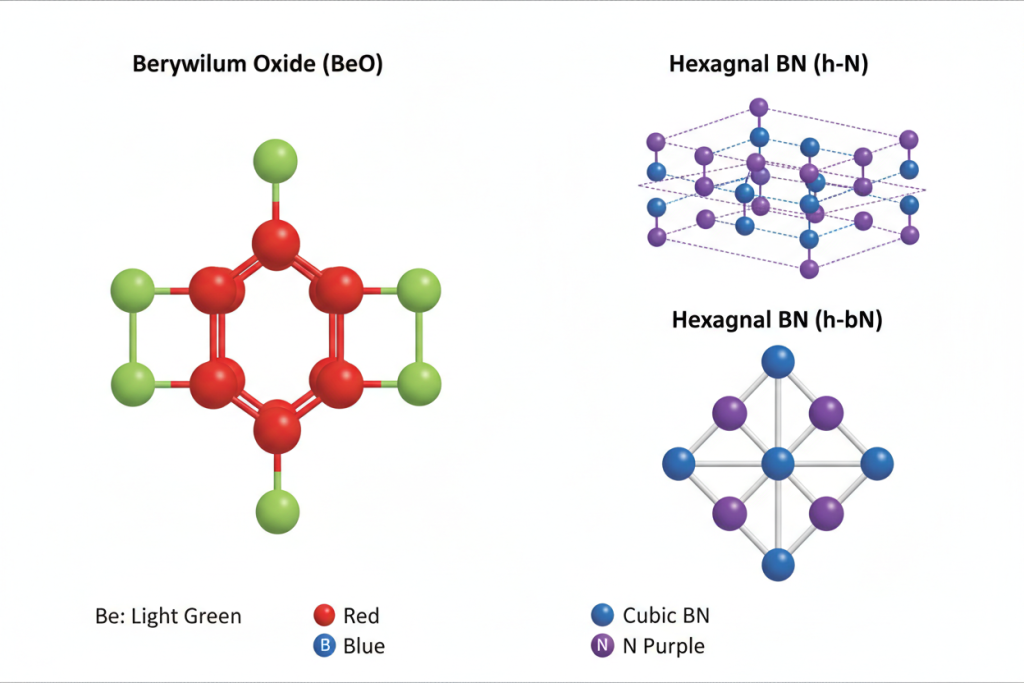
Think of Beryllium Oxide (BeO) as a massive, multi-lane copper highway for heat. It moves thermal energy away from your components faster than almost any other electrically insulating material on earth (second only to diamond). However, this highway requires “hazmat-level” clearance to build or repair. If the material fractures, or if you need to drill a hole, the resulting dust is highly toxic.
On the other hand, Boron Nitride (BN) is like a slightly narrower highway. It doesn’t move heat quite as fast as BeO, but it is completely safe to handle, incredibly easy to navigate (machine), and highly adaptable to complex terrain (intricate board shapes). BN is often referred to as “white graphite” because of its soft, lubricious nature, making it a dream for mechanical processing.
Core Concept Comparison Table
| Feature | Beryllium Oxide (BeO) | Boron Nitride (BN) |
|---|---|---|
| Primary Advantage | Unmatched thermal conductivity (~250-300 W/m·K). | Excellent machinability, safe handling, low Dk. |
| Primary Drawback | Highly toxic dust during machining (Berylliosis risk). | Lower thermal conductivity compared to BeO. |
| Machinability | Extremely hard, brittle; requires diamond tooling. | Soft, “graphite-like”; easily milled and drilled. |
| Toxicity / Safety | High Risk: Requires extreme safety protocols. | Zero Risk: Non-toxic, standard handling. |
| Ideal Application | Legacy military, high-power lasers, extreme heat zones. | RF/Microwave, complex shaped PCBs, prototyping. |
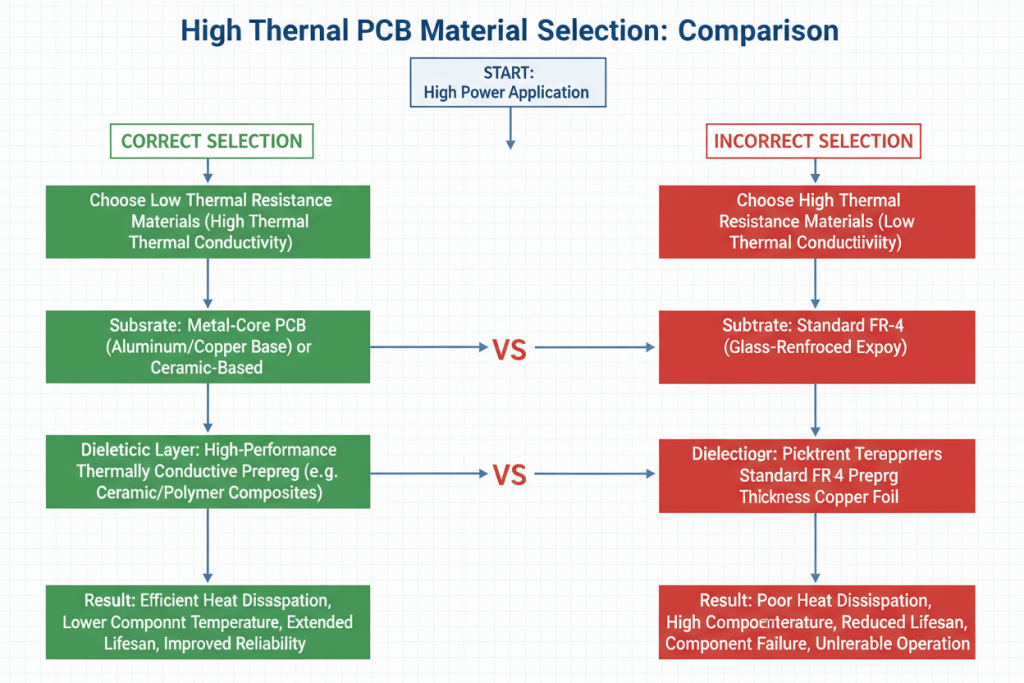
Material Specifications & Real-World Selection Guide
When selecting a substrate, hardware engineers must rely on hard data. Below is a comprehensive specification table comparing BeO and BN, followed by a deep dive into what these numbers mean for your PCB design.
Technical Specification Data Sheet
| Specification | Beryllium Oxide (BeO) | Boron Nitride (Hexagonal BN) |
|---|---|---|
| Thermal Conductivity (W/m·K) | 250 – 300 | 30 – 120 (Direction dependent) |
| Dielectric Constant (Dk @ 1MHz) | 6.7 | 4.0 |
| Dissipation Factor (Df @ 1MHz) | 0.0004 | 0.0002 |
| Coefficient of Thermal Expansion (CTE) | 8.0 – 9.0 ppm/°C | 1.0 – 4.0 ppm/°C |
| Hardness (Mohs Scale) | 9 (Extremely Hard) | 2 (Very Soft) |
| Volume Resistivity (Ω·cm) | > 10^14 | > 10^14 |
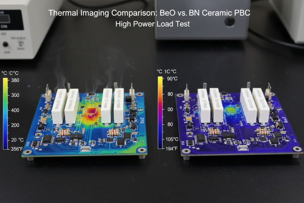
Thermal Conductivity & Heat Dissipation
Thermal conductivity dictates how efficiently a material transfers heat. BeO dominates this category with a staggering 250-300 W/m·K, making it the default choice for high-power semiconductor packaging where space is minimal and heat generation is extreme.
However, BN offers a respectable 30-120 W/m·K. While lower than BeO, it is still vastly superior to standard FR4 (0.2 W/m·K) and often competes well when comparing Silicon Nitride vs Alumina for power electronics. For many mid-to-high power applications, BN provides more than enough thermal headroom without the associated toxicity.
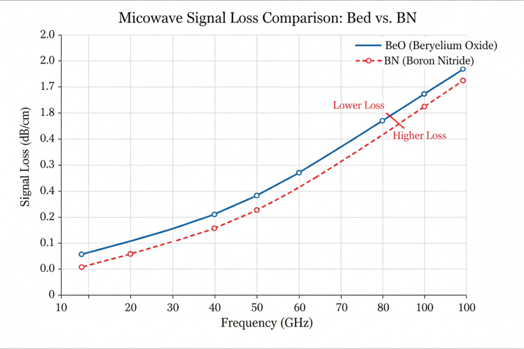
Dielectric Performance for RF/Microwave
In high-frequency applications (RF, microwave, millimeter-wave), thermal management is only half the battle. Signal integrity is paramount.
- Dielectric Constant (Dk): A measure of how much electrical energy a material stores. In high-speed electronics, a lower Dk prevents signal delay and loss. BN shines here with a Dk of ~4.0, significantly outperforming BeO (6.7).
- Dissipation Factor (Df): BN also boasts an exceptionally low loss tangent, meaning very little signal is lost as heat. For high-frequency radar or communication arrays, BN is often the superior electrical choice.
Machinability, Mechanical Strength, and HDI Integration
Modern PCB designs often require High Density Interconnects (HDI). Implementing HDI PCB integration on ceramics involves laser-drilling microvias and routing complex shapes.
- BeO: Because of its extreme hardness (Mohs 9) and brittleness, machining BeO is expensive and slow. Furthermore, any laser drilling or cutting vaporizes the material, requiring highly specialized, enclosed hazmat facilities to capture the toxic dust.
- BN: Hexagonal BN is soft and easily machinable with standard carbide tooling. You can drill precise microvias, mill complex cavities, and shape the board without specialized environmental controls. This drastically reduces tooling wear, manufacturing time, and overall prototyping costs.
The Elephant in the Room: Toxicity and Manufacturing Safety
The primary reason the electronics industry is actively seeking alternatives to Beryllium Oxide is Berylliosis, officially known as Chronic Beryllium Disease (CBD).
CBD is a severe, incurable, and potentially fatal lung disease caused by inhaling Beryllium Oxide dust. It is crucial to understand that solid BeO ceramics are perfectly safe to handle. You can touch a finished BeO PCB without risk. The danger arises entirely during the manufacturing and assembly phases:
- Cutting, scoring, or snapping the ceramic substrate.
- Drilling vias or microvias.
- Laser profiling or sanding the edges.
- Accidental fracturing of the board during mounting or extreme vibration.
Because of this, facilities that process BeO must adhere to rigorous OSHA regulations, utilizing negative-pressure cleanrooms, heavy-duty HEPA filtration, and full-body hazmat suits for workers. These safety overheads are directly passed onto the consumer, making BeO PCBs exceptionally expensive. Furthermore, end-of-life disposal of BeO components is heavily regulated in the EU (under RoHS/REACH equivalents) and the US, adding hidden lifecycle costs.
Boron Nitride completely bypasses these issues. It is non-toxic, environmentally benign, and requires no special handling, making it highly attractive for modern, compliance-focused engineering teams.

Expert Tips & Common Pitfalls to Avoid
Drawing from ongoing discussions among hardware engineers on platforms like Reddit (r/PrintedCircuitBoard) and industry forums, here are the most common pitfalls when choosing between BeO and BN:
- Pitfall 1: Blindly Over-Specifying BeO: Many engineers default to BeO simply because it has the highest thermal conductivity number on the chart. Expert Tip: Conduct a thorough thermal simulation. If your heat dissipation requirement is under 120 W/m·K, Boron Nitride or Aluminum Nitride will save you massive amounts of money and compliance headaches.
- Pitfall 2: Ignoring the CTE Mismatch: The Coefficient of Thermal Expansion (CTE) dictates how much the PCB expands when heated. If the PCB expands faster than the silicon chip attached to it, the solder joints will shear off. Expert Tip: BN has a lower CTE (1.0 – 4.0 ppm/°C) that closely matches silicon, reducing thermal stress on heavy components during rapid temperature cycling.
- Pitfall 3: Forgetting End-of-Life Liabilities: Defense contractors often specify BeO for legacy systems. However, new commercial aerospace or telecommunications projects must consider disposal. Expert Tip: Always factor in the cost of hazardous waste disposal when calculating the total ROI of a BeO board.
Conclusion
Choosing the right high-thermal ceramic substrate requires looking at the entire lifecycle of your product—from electrical performance to manufacturing safety.
Beryllium Oxide remains the undisputed champion of raw thermal conductivity, making it indispensable for specific, extreme-heat legacy applications. However, its severe toxicity risks and exorbitant machining costs make it a liability for modern, fast-paced development. Boron Nitride emerges as a highly capable, safe, and electrically superior alternative, particularly for high-frequency RF/microwave applications that require complex HDI routing.