How to Master High-Speed Industrial Motherboard PCB Assembly: Design & Routing Considerations
Designing a motherboard for an air-conditioned server room is challenging. Designing that same high-speed motherboard to operate flawlessly inside a vibrating CNC machine, a dusty factory floor, or an outdoor telecom enclosure is an entirely different beast. For hardware engineers and system architects, the intersection of high-speed digital signals (PCIe Gen 4/5, DDR4/5) and harsh industrial environments creates a perfect storm of Signal Integrity (SI) and Electromagnetic Interference (EMI) anxiety. A single impedance mismatch or microvia failure can lead to catastrophic downtime. In this comprehensive guide, we will break down the critical design considerations for high-speed industrial motherboard PCB assembly, from stackup design and thermal management to advanced BGA inspection, ensuring your next industrial PCBA survives where standard boards fail.
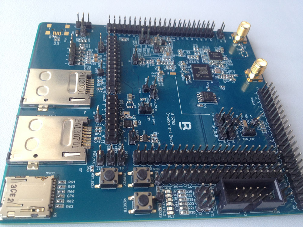
Understanding High-Speed Industrial Motherboard PCBA: The Basics
In the consumer electronics world, a motherboard is designed for a controlled environment with a lifespan of perhaps three to five years. In the industrial sector—encompassing factory automation, robotics, aerospace, and energy infrastructure—motherboards are subjected to extreme temperature cycling, high-frequency vibrations, corrosive chemicals, and severe electromagnetic noise.
When you introduce high-speed interfaces into this environment, the physics of the board change. At Gigabit speeds, PCB traces no longer act like simple wires; they become transmission lines. Every via, every bend in a trace, and every change in the dielectric material can cause signal reflections, attenuation, and jitter.
For B2B procurement managers and hardware designers in North America and Europe, the stakes are incredibly high. Industrial systems demand IPC-A-610 Class 3 compliance—the strictest standard for electronic assembly, mandating that the equipment must provide continuous performance in critical environments where downtime is unacceptable. To achieve this, you need more than just a standard manufacturer; you need a reliable PCBA partner capable of bridging the gap between advanced signal integrity engineering and ruggedized mechanical design.
Core Concepts Simplified
To make informed decisions during the design and procurement phases, it is crucial to understand the underlying physics of high-speed industrial boards. Here are the core concepts, translated from deep engineering jargon into practical analogies.
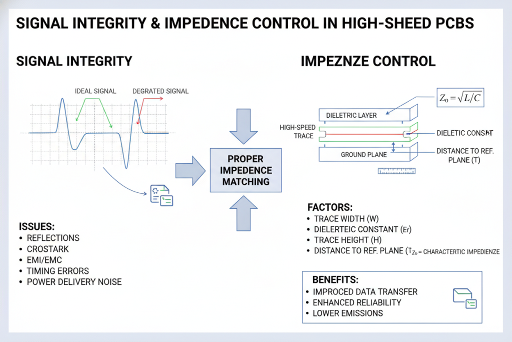
Signal Integrity (SI) and Controlled Impedance
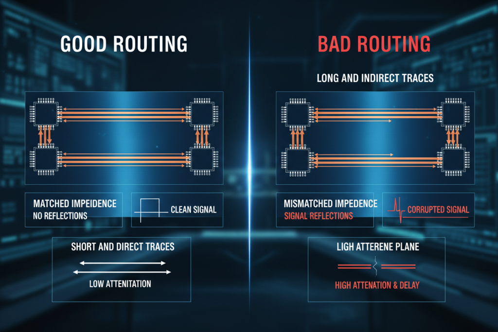
Imagine high-speed digital signals as water flowing at high pressure through a network of pipes. Controlled Impedance ensures that the “pipe” (the PCB trace) maintains a perfectly consistent diameter from the source to the destination. If the trace suddenly widens or narrows, or if it changes layers without proper grounding, it causes a “water hammer” effect. The signal violently bounces back (reflection), scrambling the data. In high-speed industrial motherboards, maintaining strict impedance control (usually ±5% to ±10%) is non-negotiable to prevent data loss.
Crosstalk Mitigation
Think of crosstalk like trying to have a serious conversation in a busy office with thin walls. Signals from neighboring wires can “talk over” each other through electromagnetic coupling. To prevent this, PCB designers must install “soundproof walls”—this means maintaining adequate spacing between high-speed differential pairs (using the 3W rule) and utilizing proper ground planes to isolate noisy signals.
Thermal Management and Power Integrity (PI)
Operating a high-speed processor in an industrial environment is like trying to cool a high-end gaming PC inside an industrial oven. Power Integrity ensures the chips get clean, stable power without voltage drops, while Thermal Management (using thermal vias, heavy copper layers, and aluminum backplates) aggressively pulls heat away from critical components like CPUs and FPGAs before they throttle or fail.
Advanced BGA Assembly and 3D AXI
Modern high-speed chips use Ball Grid Array (BGA) packaging, where the solder connections are hidden underneath the chip. Visual inspection is useless here. 3D Automated X-Ray Inspection (AXI) acts as an MRI scan for your industrial motherboard. It slices through the layers visually to ensure there are no hidden air bubbles (voiding) or micro-cracks in the solder joints, which would inevitably fail under industrial vibration.
Comparison: Standard vs. High-Speed Industrial Motherboards
| Feature / Metric | Standard Commercial Motherboard | High-Speed Industrial Motherboard | Impact on Performance |
|---|---|---|---|
| PCB Material | Standard FR-4 (High loss at high frequency) | Mid-loss to Ultra-low loss (e.g., Megtron 6, Rogers) | Prevents high-frequency signal degradation. |
| Assembly Standard | IPC-A-610 Class 2 | IPC-A-610 Class 3 | Ensures zero-downtime reliability in harsh conditions. |
| BGA Inspection | 2D X-Ray (Sample basis) | 100% 3D AXI (Automated X-Ray Inspection) | Guarantees solder joint integrity against vibration. |
| Thermal Strategy | Basic heatsinks, active fans | Heavy Copper (2oz-4oz), Thermal Vias, Conformal Coating | Survives extreme ambient temperatures without active cooling. |
| Impedance Control | ±10% to ±15% tolerance | Strict ±5% to ±8% tolerance | Eliminates data scrambling in PCIe and DDR interfaces. |
Step-by-Step Guide: Designing for Manufacturability (DFM)
Designing a high-speed industrial motherboard requires a methodical approach. Here is a highly technical, actionable framework to ensure your design is both high-performing and manufacturable.
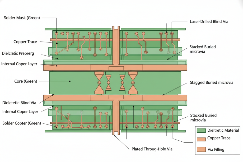
Step 1: Architecting the Layer Stackup
The foundation of Signal Integrity is the PCB stackup. For industrial motherboards handling PCIe Gen 4/5 or DDR5, a standard 4-layer or 6-layer board is insufficient. You will typically need an 8-layer to 14-layer High-Density Interconnect (HDI) structure.
- Material Selection: Move away from standard FR4. Specify materials with a low Dielectric Constant (Dk) and low Loss Tangent (Df), such as Panasonic Megtron 6 or Isola I-Speed.
- Symmetrical Design: Ensure the stackup is perfectly symmetrical from the core outward to prevent the board from warping inside the reflow oven.
- Grounding: Every high-speed signal layer must be directly adjacent to a solid, unbroken ground plane to provide a clear return path and contain EMI.
Step 2: Routing High-Speed Interfaces
When routing traces for high-speed components, adherence to strict geometric rules is required.
- Length Matching: Differential pairs (like TX/RX in PCIe) must be length-matched to within mils to prevent timing skew.
- Avoid 90-Degree Angles: Sharp corners cause impedance variations and act as EMI antennas. Use 45-degree angles or smooth arcs.
- Via Minimization: Every via introduces parasitic capacitance and inductance. Route critical signals on the same layer whenever possible. If vias are necessary, use blind or buried microvias and include ground return vias nearby.
Step 3: Implementing Ruggedization Techniques
Industrial environments destroy fragile electronics. Your assembly process must include ruggedization.
- Underfill: Apply an epoxy underfill beneath massive BGA components (like CPUs or FPGAs). This mechanically bonds the chip to the PCB, absorbing mechanical shock and thermal expansion stress that would otherwise crack the solder balls.
- Conformal Coating: Specify a conformal coating (Acrylic, Silicone, or Polyurethane) to protect the exposed traces and SMD components from moisture, conductive dust, and chemical vapors.
High-Speed Industrial PCBA Specifications Data
| Specification Category | Recommended Industrial Standard | Critical Rationale |
|---|---|---|
| Operating Temperature | -40°C to +85°C (Industrial Grade) | Ensures components do not fail or drift in spec during extreme weather or factory heat. |
| Vibration Resistance | MIL-STD-810G or IEC 60068-2-6 | Prevents mechanical failure of heavy components (capacitors, inductors, BGAs). |
| Surface Finish | ENIG (Electroless Nickel Immersion Gold) | Provides a perfectly flat surface for fine-pitch BGAs and excellent oxidation resistance. |
| Copper Weight | 2 oz to 4 oz on inner power layers | Handles high-current industrial power supplies without localized overheating. |
| Cleanliness Standard | < 1.56 µg/cm² NaCl equivalent | Prevents dendritic growth and shorts in high-humidity environments. |
Expert Tips & Common Pitfalls to Avoid
Drawing from real-world post-mortems and discussions on platforms like Reddit (r/PrintedCircuitBoard) and EEVblog, here are the most common traps engineers fall into when designing high-speed industrial boards—and how to avoid them.
Pitfall 1: Trusting the Auto-Router for High-Speed Signals
The Mistake: Using EDA software auto-routers to save time on complex DDR or PCIe routing.
The Reality: Auto-routers do not understand the nuances of return paths or crosstalk. They will happily route a high-speed trace over a split in the ground plane, instantly ruining your signal integrity and causing massive EMI emissions.
The Fix: Manually route all critical high-speed interfaces. Verify the continuous ground return path visually. If a trace crosses a split plane, you must provide stitching capacitors.
Pitfall 2: Ignoring Fiberglass Weave Skew
The Mistake: Assuming the PCB substrate is a perfectly uniform material.
The Reality: Standard PCB dielectrics are made of woven fiberglass cloth soaked in epoxy. At ultra-high speeds (10 Gbps+), if one trace of a differential pair sits over a glass bundle and the other sits over epoxy, they experience different dielectric constants. One signal travels faster than the other, causing “skew” and data corruption.
The Fix: For ultra-high-speed industrial boards, specify tightly woven glass (like 1080 or 106 weave) or route the high-speed traces at a slight angle (e.g., 10 degrees) relative to the board’s X/Y axis so both traces experience the same average material.
Pitfall 3: Overlooking BGA Voiding Limits
The Mistake: Accepting standard IPC Class 2 voiding limits for BGA solder joints.
The Reality: In a desktop PC, a 25% void (air bubble) inside a BGA solder ball might be acceptable. In an industrial machine experiencing constant 50Hz vibration, that void is a stress concentrator. It will eventually crack, causing intermittent failures that are impossible to diagnose.
The Fix: Mandate strict voiding limits (<10%) with your EMS provider and demand 3D X-Ray reports for all complex BGAs. This level of quality control is a hallmark of precision PCB assembly, ensuring your industrial boards mirror the reliability of medical or aerospace equipment.
Conclusion & Final Thoughts
Designing and assembling a high-speed industrial motherboard is a balancing act. You are constantly trading off between signal integrity requirements (which favor thin traces and specific materials) and ruggedization requirements (which favor robust structures and heavy copper).
Success in this space requires moving beyond basic PCB layout. It demands rigorous stackup planning, meticulous impedance control, aggressive thermal management, and a manufacturing process strictly aligned with IPC Class 3 standards. By understanding the physics of high-speed signals and the mechanical realities of the industrial floor, you can engineer motherboards that deliver zero downtime.
Ultimately, the most critical decision is selecting the right manufacturing partner. A design is only as good as the facility that builds it. Ensure your PCBA provider has the advanced AXI inspection tools, the impedance testing capabilities (TDR), and the engineering expertise to bring your high-speed industrial concepts to life.