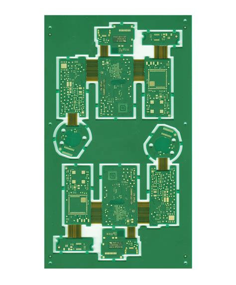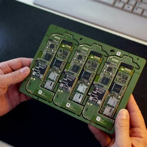
Top PCB Prototype Services for Quality and Affordability
Explore the top PCB prototype services that balance quality and affordability. Discover trusted manufacturers that cater to hobbyists and professionals alike, ensuring your projects are brought to life with precision and care.