Advanced Strategies for Precision PCB SMD Assembly Success
“Master precision PCB SMD assembly with expert techniques for component placement, soldering optimization, and thermal management to ensure flawless high-density circuit board performance.”
“Master precision PCB SMD assembly with expert techniques for component placement, soldering optimization, and thermal management to ensure flawless high-density circuit board performance.”
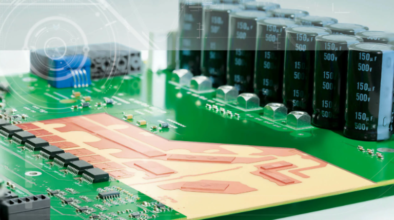
“Discover professional techniques for EGS002 inverter layouts in high-power designs (1kW+). Learn PCB optimization, thermal management, and SPWM integration best practices for maximum efficiency.”
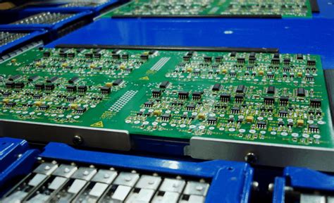
“Explore expert techniques for achieving flawless PCB board assembly, focusing on precision component placement, soldering accuracy, quality control protocols, and automated inspection systems for aerospace, medical, and consumer electronics applications.”
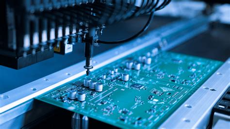
“Discover how SMT PCB assembly revolutionizes manufacturing through automated processes, precision component placement, and minimized errors, enhancing production speed while reducing operational costs.”
Introduction Printed Circuit Boards (PCBs) are essential components in modern electronics, providing mechanical support and electrical connections for electronic components….
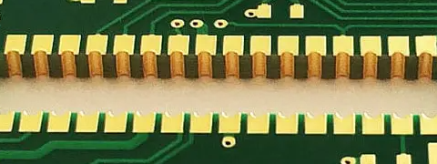
Introduction to PCB Edge Plating Printed Circuit Board (PCB) edge plating, also known as border plating or castellation, is a…
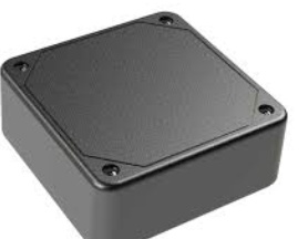
Introduction to PCB Boxes Printed Circuit Board (PCB) boxes, also known as PCB enclosures or electronic enclosures, are protective housings…
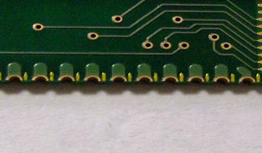
Introduction to Castellated PCBs Castellated printed circuit boards (PCBs) represent a specialized design approach that enables modular electronics assembly and…
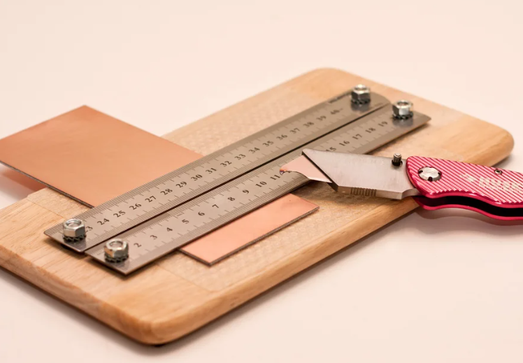
Introduction to Circuit Board Cutting In the world of electronics manufacturing, prototyping, and repair, circuit board cutters have become indispensable…

Introduction to PCB Routing Printed Circuit Board (PCB) routing is a critical step in the design and manufacturing of electronic…

“Explore the world’s largest PCB manufacturers spearheading electronics innovation. Discover 2023’s top industry leaders, their breakthroughs, and competitive edge in advanced circuit board technologies.”

“Explore 2023’s top global PCB manufacturers driving electronics innovation. Compare leading firms from China, Taiwan, and beyond in rigid, flexible, and HDI PCB production. Discover market leaders shaping tech evolution.”
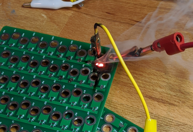
Introduction Printed Circuit Boards (PCBs) are the backbone of modern electronics, providing mechanical support and electrical connectivity for components. While…
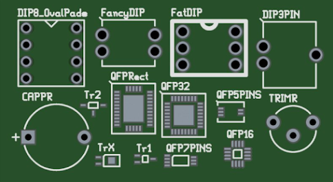
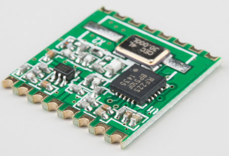
Introduction to PCB Footprints Printed Circuit Board (PCB) footprints, also known as land patterns, are essential elements in electronic design…
Introduction to PCB Footprints Printed Circuit Board (PCB) footprints, also known as land patterns, are essential elements in electronic design…
We use cookies to improve your experience on our site. By using our site, you consent to cookies.
Manage your cookie preferences below:
Essential cookies enable basic functions and are necessary for the proper function of the website.
Statistics cookies collect information anonymously. This information helps us understand how visitors use our website.
Google Analytics is a powerful tool that tracks and analyzes website traffic for informed marketing decisions.
Service URL: policies.google.com (opens in a new window)
SourceBuster is used by WooCommerce for order attribution based on user source.
You can find more information in our privacy policy and privacy policy.