additive pcb | additive pcb manufacturing | advanced assembly pcb | advanced circuit board | advanced circuits 4pcb | advanced circuits assembly | advanced circuits barebones | advanced circuits flex pcb | advanced circuits pcb | advanced circuits pcb artist | advanced circuits quote | advanced pcb manufacturing | advanced printed circuit technology | aerospace pcb assembly | uncategories
A brief discussion on why PCB size expands and shrinks and solutions
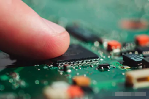
During the PCB processing process, from the transfer of the inner layer circuit pattern of the PCB substrate to several times of lamination until the transfer of the outer layer circuit pattern, the panel will expand and shrink in different directions in the warp and weft. From the entire PCB production FLOW-CHART, we can find…