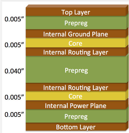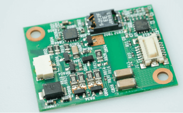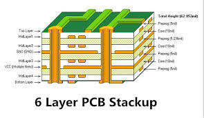
6-layer pcb stackup
he best practices for 6-layer PCB stacking design include reasonable hierarchy, optimized signal layer layout, good power and grounding design, appropriate use of vias, and effective thermal management. By following these best practices, the performance and reliability of the circuit board can be significantly improved to meet the needs of high-performance applications.