uncategories

  • Equipment involved in pcb manufacturing

    Printed Circuit Board (PCB) prototyping is a critical phase in the development of electronic devices, serving as the bridge between conceptual design and mass production. The process involves a series of steps that require precision and accuracy, necessitating the use of specialized equipment. Understanding the essential tools involved in PCB prototyping is crucial for ensuring the quality and functionality of the final product.

  • Embedded copper coin pcb

    Embedded copper coin PCBs have emerged as a pivotal innovation in the realm of high-power applications, offering a multitude of benefits that address the growing demands for efficiency, reliability, and thermal management. As electronic devices continue to evolve, the need for robust solutions that can handle increased power densities without compromising performance has become paramount. Embedded copper coin PCBs, with their unique construction and material properties, provide an effective answer to these challenges.

  • |

    Dynamic flex pcb

    Dynamic flex PCB, or flexible printed circuit boards, have become increasingly integral to the advancement of modern electronics. These innovative components offer a multitude of advantages that make them indispensable in various applications, ranging from consumer electronics to industrial machinery. One of the primary benefits of dynamic flex PCBs is their inherent flexibility, which allows for more compact and versatile designs. Unlike traditional rigid PCBs, dynamic flex PCBs can be bent, folded, and twisted without compromising their functionality. This flexibility enables designers to create more intricate and space-efficient electronic devices, which is particularly valuable in the development of wearable technology, medical devices, and compact consumer electronics.

  • |

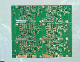
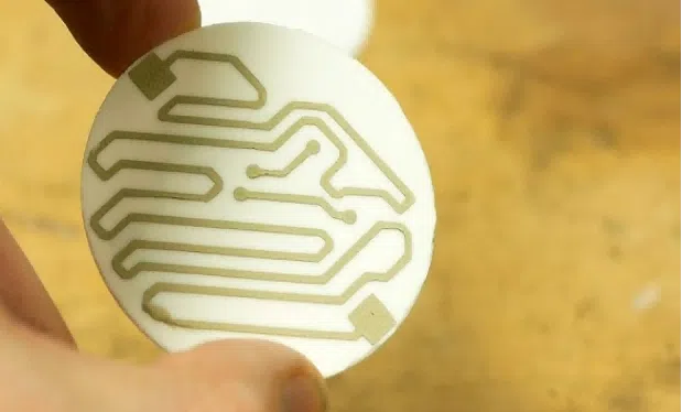
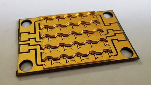
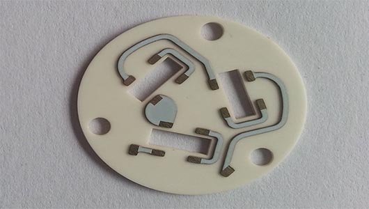
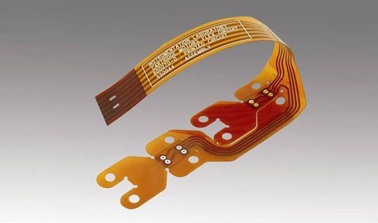
    Double sided flex pcb

    Double sided flexible printed circuit boards (PCBs) have become increasingly integral to the advancement of modern electronics, offering a multitude of advantages that cater to the evolving demands of contemporary technology. These PCBs, characterized by their ability to accommodate conductive pathways on both sides of a flexible substrate, present a unique combination of flexibility, durability, and efficiency that traditional rigid PCBs cannot match.

  • Double sided aluminum pcb

    Advantages Of Double Sided Aluminum PCB In LED Applications Double-sided aluminum PCBs have emerged as a pivotal component in the realm of LED applications, offering a multitude of advantages that enhance performance, reliability, and efficiency. These printed circuit boards, characterized by their aluminum core and conductive layers on both sides, are particularly well-suited for high-power…

  • Diy pcb assembly

    Embarking on the journey of DIY PCB assembly can be both a rewarding and educational experience. To ensure a successful project, it is essential to follow a systematic approach. The first step involves designing the PCB layout using specialized software such as Eagle, KiCad, or Altium Designer. These tools allow you to create a schematic diagram, which serves as a blueprint for your circuit. Once the schematic is complete, you can proceed to design the PCB layout, ensuring that all components are correctly placed and connected.

  • Diy multilayer pcb

    Designing your own multilayer printed circuit board (PCB) can be a rewarding endeavor, offering both the satisfaction of creating a custom solution and the potential for significant cost savings. To embark on this journey, it is essential to understand the step-by-step process involved in creating a multilayer PCB, from initial design to final production. This guide aims to provide a comprehensive overview of the necessary steps, ensuring a smooth and successful project.

  • Digital high speed pcb application

    In the realm of digital high-speed printed circuit board (PCB) design, optimizing signal integrity is paramount to ensuring the reliable performance of electronic systems. As data rates continue to escalate, the challenges associated with maintaining signal integrity become increasingly complex. Consequently, designers must employ a variety of strategies to mitigate issues such as signal degradation, crosstalk, and electromagnetic interference (EMI).

  • Design high speed pcb

    Designing high-speed printed circuit boards (PCBs) is a complex task that requires meticulous attention to detail and a deep understanding of both electrical and mechanical principles.

    As technology advances, the demand for faster and more efficient electronic devices continues to grow, making the need for high-speed PCB design more critical than ever. To achieve optimal performance, it is essential to follow best practices that ensure signal integrity, minimize electromagnetic interference (EMI), and maintain overall system reliability.

  • Design flex pcb

    Advantages Of Using Flexible PCBs In Modern Electronics In the ever-evolving landscape of modern electronics, the demand for more compact, efficient, and versatile devices has led to significant advancements in the design and implementation of printed circuit boards (PCBs). Among these innovations, flexible PCBs, or flex PCBs, have emerged as a game-changer, offering a myriad…

  • Design custom pcb

    Designing a custom printed circuit board (PCB) is a meticulous process that requires careful planning and execution. The journey begins with a clear understanding of the project requirements, which involves defining the functionality, size, and shape of the PCB. This initial phase is crucial as it sets the foundation for the entire design process. Once the requirements are established, the next step is to create a schematic diagram. This diagram serves as a blueprint, illustrating how different components will be connected. It is essential to ensure that the schematic is accurate and comprehensive, as any errors at this stage can lead to significant issues later on.

  • ceramic substrate for pcb

    When it comes to designing printed circuit boards (PCBs), the choice of substrate material can make a world of difference. While traditional materials like FR4 have been the go-to for many years, ceramic substrates are increasingly gaining traction. So, why are more and more engineers and designers opting for ceramic substrates in PCB design? Let’s dive into the advantages and see what all the buzz is about.

  • Ceramic pcb thickness

    Importance Of Ceramic PCB Thickness In High-Frequency Applications When it comes to high-frequency applications, the thickness of ceramic PCBs (Printed Circuit Boards) is a crucial factor that can significantly impact performance. You might be wondering why this is the case. Well, let’s dive into the nitty-gritty of why ceramic PCB thickness matters so much in…

  • ceramic pcb soldering

    ceramic PCB Soldering can be a bit of a challenge, but with the right techniques, it’s totally doable. Ceramic PCBs, known for their excellent thermal conductivity and electrical insulation, are increasingly popular in high-power and high-frequency applications. However, their unique properties also mean that traditional soldering methods might not always work. So, let’s dive into some effective techniques for soldering ceramic PCBs.

  • Ceramic pcb prototype

    When it comes to high-frequency applications, the choice of materials can make or break the performance of your electronic devices.

    One material that’s been gaining a lot of traction lately is ceramic, particularly in the form of ceramic PCB prototypes. You might be wondering why ceramic is becoming the go-to material for these applications. Well, let’s dive into the advantages and see why ceramic PCB prototypes are making waves in the tech world.