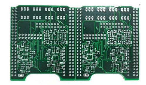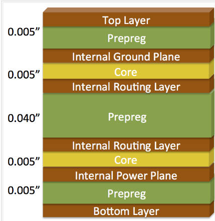
6 layer pcb stackup for high speed
6 layer pcb stackup for high speed y applications requires comprehensive consideration of multiple factors such as signal integrity, power stability, and electromagnetic compatibility. Excellent performance of high-frequency circuits can be ensured through reasonable stacking structure, fine signal layout, tight power and ground coupling, careful use of vias, and effective simulation and testing.simulation and testing.