
Ceramic PCB Manufacturing Process: DBC, AMB, and LTCC Explained
If you need to select the right ceramic PCB manufacturing process for your high-power electronics project, then you will need to understand the fundamental differences between Direct Bonded Copper (DBC), Active Metal Brazing (AMB), and Low Temperature Co-fired Ceramic (LTCC) technologies, including their thermal performance, design constraints, and cost implications.
Ceramic substrates deliver thermal conductivity up to 400 times higher than standard FR-4 PCBs, with alumina reaching 24-28 W/mK and aluminum nitride achieving 150-230 W/mK compared to FR-4’s 0.4 W/mK. According to power electronics industry analysis, inadequate thermal management causes approximately 55% of failures in high-power applications. Selecting the appropriate ceramic manufacturing process—DBC, AMB, or LTCC—determines whether your design achieves reliable performance or encounters thermal limitations and excessive costs.
This technical guide examines three primary ceramic PCB manufacturing processes used in power electronics, RF systems, and high-reliability applications. You will learn how each process bonds copper to ceramic substrates, their respective thermal and mechanical properties, design rule requirements, and application-specific selection criteria.
What is Ceramic PCB Manufacturing?
Ceramic PCB manufacturing is the process of forming conductive circuit layers on rigid inorganic ceramic substrates using high-temperature bonding, vacuum deposition, or screen-printing techniques. Unlike organic PCBs that use epoxy-glass laminates, ceramic PCBs utilize alumina (Al₂O₃), aluminum nitride (AlN), or silicon nitride (Si₃N₄) substrates that provide exceptional thermal conductivity, electrical insulation, and dimensional stability under extreme temperatures.
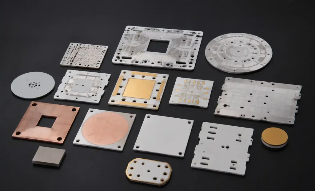
The manufacturing process selection depends on substrate material compatibility, required copper thickness, circuit complexity, and thermal performance targets. DBC and AMB processes create thick copper layers (0.2-0.8mm) suitable for high-current power electronics, while LTCC enables complex multilayer structures with embedded passive components for RF and microwave applications.
You should specify ceramic PCB manufacturing when your application requires operating temperatures above 150°C, thermal conductivity exceeding 20 W/mK, high voltage isolation beyond 3kV, or coefficient of thermal expansion (CTE) matching with semiconductor devices. Automotive power inverters, LED lighting systems, RF amplifiers, and aerospace electronics commonly use ceramic substrates due to superior reliability under thermal stress.
Direct Bonded Copper (DBC) Process
Direct Bonded Copper technology bonds copper foil directly to ceramic substrates through a eutectic oxidation reaction at temperatures between 1065-1083°C. The process forms a copper-oxygen-ceramic interface that creates a strong metallurgical bond without requiring intermediate brazing materials or adhesives.
DBC Manufacturing Process Steps
The DBC process begins with high-purity copper foil (typically 99.9% Cu) placed on a cleaned ceramic substrate in an oxygen-containing atmosphere. At temperatures approaching copper’s melting point, a thin copper oxide (Cu₂O) layer forms at the interface. This eutectic mixture wets the ceramic surface and reacts with alumina to create a permanent bond as the assembly cools.
Process control requires precise temperature management within ±10°C and careful oxygen concentration to ensure uniform oxide formation. The bonded assembly undergoes cooling at controlled rates to minimize thermal stress from CTE mismatch between copper (17 ppm/°C) and alumina (6.5-7.2 ppm/°C). After bonding, the copper layer is patterned using standard photolithography and etching processes.
DBC technology works exclusively with alumina substrates because the process requires specific chemical interaction between copper oxide and Al₂O₃. You cannot use DBC for aluminum nitride or silicon nitride ceramics—these materials require AMB technology instead.
DBC Technical Specifications
| Parameter | Specification | Notes |
|---|---|---|
| Substrate Material | Al₂O₃ (96% or 99.6%) | DBC exclusive to alumina |
| Copper Thickness | 0.2-0.8mm (200-800μm) | Standard: 0.3mm, 0.4mm |
| Bond Strength | >20 MPa (typical 25-30 MPa) | Per IPC-TM-650 peel test |
| Processing Temperature | 1065-1083°C | Eutectic bonding range |
| Thermal Conductivity | 24-28 W/mK (substrate) | Alumina dependent |
| Maximum Board Size | Up to 300mm × 400mm | Manufacturer dependent |
The copper layer thickness in DBC substrates typically ranges from 0.2-0.8mm, significantly thicker than standard PCB copper (0.035-0.105mm or 1-3 oz). This heavy copper capability enables high current handling for power electronics applications where components dissipate 50-500W or more.
DBC Applications and Design Considerations
DBC substrates dominate power electronics applications due to excellent thermal performance combined with lower cost than AMB technology. You should specify DBC ceramic when your design requires alumina substrates and can accept the thermal conductivity limitations of Al₂O₃ compared to AlN or Si₃N₄.
Primary Applications:
- IGBT and MOSFET power modules (automotive, industrial)
- Solar inverters and wind power converters
- Induction heating systems
- Medium-power LED arrays
- Electric vehicle charging stations
You will need to consider thermal expansion mismatch when designing DBC assemblies. The 10-11 ppm/°C difference between copper and alumina creates mechanical stress during thermal cycling. Design guidelines recommend minimum feature sizes of 0.5mm for traces and spacing, with 1-2mm edge clearance from board edges to prevent delamination.
Active Metal Brazing (AMB) Process
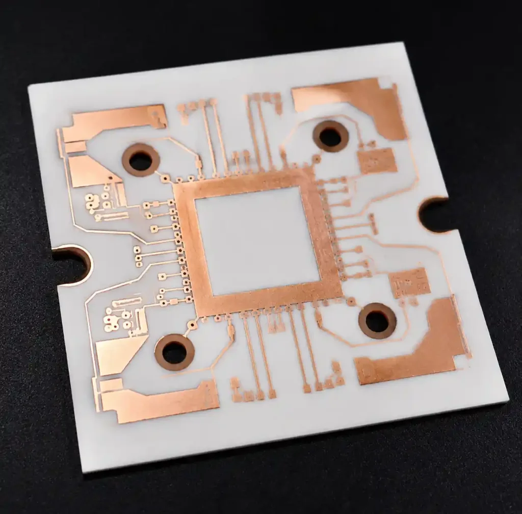
Active Metal Brazing bonds copper to ceramic substrates using a brazing alloy containing active metals—typically titanium, zirconium, or hafnium—that chemically react with nitride ceramics to form strong metallurgical bonds. AMB technology enables copper bonding to aluminum nitride (AlN) and silicon nitride (Si₃N₄), which cannot be processed using DBC.
AMB Manufacturing Process Details
The AMB process uses silver-copper-titanium (Ag-Cu-Ti) brazing alloys with compositions typically containing 1-5% titanium. During brazing at 800-900°C under vacuum (10⁻⁵ to 10⁻⁶ mbar), the active titanium element diffuses to the ceramic interface and forms titanium nitride (TiN) and titanium silicide (Ti₅Si₃) compounds with Si₃N₄ substrates, or titanium nitride layers with AlN.
These reaction layers create a true chemical bond that survives severe thermal cycling regimes where DBC alumina substrates would experience bond degradation. The brazing process occurs at lower temperatures (800-900°C) compared to DBC (1065-1083°C), reducing thermal stress on the ceramic substrate.
Process quality depends on vacuum level, brazing temperature profile, alloy composition, and time at temperature. Insufficient vacuum or temperature deviations produce incomplete bonding, while excessive temperature or time can cause titanium depletion and weak joints. Manufacturing tolerances typically maintain bond strength above 25-35 MPa.
AMB Technical Specifications
| Parameter | Specification | Notes |
|---|---|---|
| Substrate Material | AlN, Si₃N₄, Al₂O₃ | Nitride ceramics primary |
| Copper Thickness | 0.2-0.8mm (200-800μm) | Heavy copper capability |
| Bond Strength | 25-35 MPa typical | Higher than DBC |
| Processing Temperature | 800-900°C | Lower than DBC |
| Thermal Conductivity | 150-230 W/mK (AlN) | 6-8× higher than DBC alumina |
| CTE Match | 4.5-5.7 ppm/°C (AlN) | Better semiconductor match |
AMB substrates using aluminum nitride achieve 150-230 W/mK thermal conductivity, approximately 6-8 times higher than DBC alumina substrates. This superior thermal performance enables power densities exceeding 500W/cm² in compact power modules where DBC technology would reach thermal limits.
AMB Applications and Design Rules
You should specify AMB ceramic substrates when your application requires maximum thermal conductivity, superior CTE matching with silicon or GaN semiconductors, or operating temperatures exceeding alumina’s capabilities. The higher cost of AMB (typically 3-5× more than DBC) is justified when thermal or reliability requirements exceed DBC capabilities.
Primary Applications:
- High-power automotive inverters (electric vehicles >200kW)
- SiC and GaN power modules (800V-1200V systems)
- Laser diode arrays and high-brightness LED systems
- Military and aerospace power electronics
- RF power amplifiers requiring thermal management
Design rules for AMB substrates follow similar guidelines to DBC, with minimum feature sizes of 0.5mm for traces and gaps. However, the superior CTE match between AlN (4.5-5.7 ppm/°C) and silicon (2.6-3.5 ppm/°C) significantly reduces thermal cycling stress on solder joints compared to alumina-based DBC substrates.
You can use AMB technology with alumina substrates when cost constraints prevent AlN selection but higher bond strength than DBC is required. AMB alumina provides a cost-performance position between standard DBC and premium AlN substrates.
Low Temperature Co-fired Ceramic (LTCC) Process
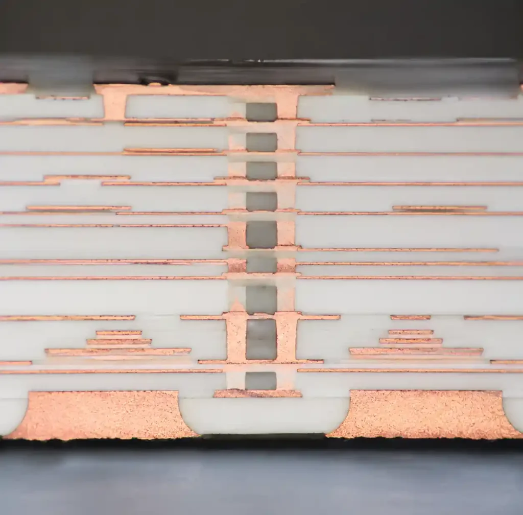
LTCC technology manufactures multilayer ceramic substrates by screen-printing conductor patterns on unfired ceramic tape sheets, stacking multiple layers with alignment, and co-firing the assembly at 850-900°C. This process enables complex three-dimensional circuit structures with embedded passive components and vertical interconnections.
LTCC Manufacturing Process Steps
LTCC fabrication begins with “green tape” ceramic sheets composed of glass-ceramic powder and organic binders. Conductor pastes containing silver, gold, or copper are screen-printed onto individual tape layers to form circuit patterns, vias, and passive components. Multiple layers are precisely aligned and laminated under heat and pressure to form a monolithic stack.
The laminated assembly undergoes a controlled firing schedule in a tunnel furnace. During firing at 850-900°C, organic binders burn out, glass phases sinter, and the ceramic powder densifies to create a solid substrate. The lower firing temperature compared to HTCC (High Temperature Co-fired Ceramic at 1500-1600°C) allows use of high-conductivity metals like silver and gold that would oxidize at higher temperatures.
Post-fire processing includes surface metallization, pad plating, and attachment of external components. LTCC substrates can integrate resistors, capacitors, and inductors within the ceramic layers, eliminating discrete surface-mount components and reducing assembly size.
LTCC Technical Specifications and Capabilities
| Parameter | Specification | Standard Values |
|---|---|---|
| Layer Count | 2-50+ layers | Typical: 8-20 layers |
| Conductor Materials | Ag, Au, Ag-Pd, Cu | Silver most common |
| Firing Temperature | 850-900°C | Material dependent |
| Via Diameter | 100-150μm minimum | Process dependent |
| Line Width/Spacing | 75-100μm minimum | Standard capability |
| Thermal Conductivity | 3-5 W/mK typical | Lower than DBC/AMB |
| Dielectric Constant | 4-10 (tunable) | Application specific |
LTCC substrates achieve moderate thermal conductivity (3-5 W/mK), significantly lower than DBC or AMB technologies but still 8-12 times higher than FR-4 PCBs. The primary advantage of LTCC is not thermal performance but rather three-dimensional integration capability, embedded passives, and hermetic packaging.
LTCC Applications and Design Considerations
You should specify LTCC manufacturing when your application requires complex multilayer RF circuits, embedded passive components, hermetic packaging, or compact three-dimensional integration that cannot be achieved with planar DBC or AMB substrates. LTCC excels in high-frequency and miniaturized systems where circuit complexity is more critical than maximum thermal conductivity.
Primary Applications:
- RF and microwave modules (wireless communication)
- Automotive radar and sensor systems
- Medical implantable devices (hermetic packaging)
- Aerospace and military electronics
- MEMS sensor packaging
Design rules for LTCC differ significantly from DBC and AMB processes. You must account for shrinkage during firing (typically 12-15% in X-Y dimensions), which requires scaling artwork accordingly. Via registration between layers maintains ±25-50μm accuracy, and minimum feature sizes are constrained by screen-printing resolution.
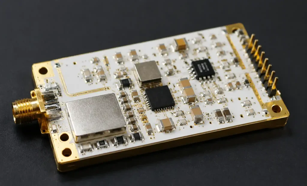
LTCC’s ability to embed resistors, capacitors, and inductors within ceramic layers enables significant size reduction for RF matching networks, filters, and DC bias circuits. This integration reduces parasitic inductances and improves high-frequency performance compared to discrete component assemblies on planar substrates.
Process Comparison and Selection Criteria
Understanding when to specify DBC, AMB, or LTCC requires evaluating thermal requirements, substrate material compatibility, circuit complexity, and cost constraints against your application’s specific performance targets.
| Selection Factor | DBC | AMB | LTCC |
|---|---|---|---|
| Substrate Materials | Al₂O₃ only | AlN, Si₃N₄, Al₂O₃ | Glass-ceramic |
| Thermal Conductivity | 24-28 W/mK | 150-230 W/mK (AlN) | 3-5 W/mK |
| Copper Thickness | 0.2-0.8mm | 0.2-0.8mm | 10-50μm (Ag/Au) |
| High Current Capability | Excellent | Excellent | Limited |
| Multilayer Complexity | Single/double-sided | Single/double-sided | 2-50+ layers |
| Embedded Passives | No | No | Yes |
| Relative Cost | 1× (baseline) | 3-5× | 2-4× |
| Lead Time | 2-4 weeks | 3-6 weeks | 4-8 weeks |
Select DBC when:
- Alumina substrate provides adequate thermal performance
- High-current power electronics require thick copper
- Cost-effectiveness is critical for production volumes
- Design is planar single or double-sided configuration
Select AMB when:
- Maximum thermal conductivity is required (AlN, Si₃N₄)
- CTE matching with semiconductors is critical for reliability
- Operating temperatures or power densities exceed DBC capabilities
- Application justifies 3-5× cost premium for superior performance
Select LTCC when:
- Complex multilayer RF circuits require 3D integration
- Embedded passive components reduce assembly size
- Hermetic packaging is required for harsh environments
- High-frequency performance and miniaturization outweigh thermal limitations
Thick Film vs Thin Film Metallization
Beyond DBC, AMB, and LTCC processes, ceramic PCB manufacturing includes thick film and thin film metallization techniques that serve distinct application requirements.
Thick Film Process
Thick film technology uses screen-printing to deposit conductor, resistor, and dielectric pastes onto ceramic substrates, followed by firing at 850-1000°C. The process creates layers 10-50μm thick with moderate resolution (line width ≥150μm) suitable for hybrid circuits and sensor applications.
Thick film conductors use silver, gold, or silver-palladium pastes that achieve 2-5 μΩ·cm resistivity—acceptable for many applications but higher than bulk copper. The process enables integrated resistors and capacitors on the same substrate, reducing component count for signal conditioning and power management circuits.
Thin Film Process
Thin film technology deposits conductor layers 0.1-10μm thick using vacuum sputtering or evaporation, then patterns them with photolithography. This semiconductor-style process achieves fine features (line width ≥25μm), tight tolerances (±1%), and excellent electrical properties.
Thin film metallization commonly uses titanium-tungsten, gold, or copper with barrier layers. Resistivity approaches bulk metal values, and dimensional accuracy enables precision analog circuits, RF components with controlled impedance, and high-density interconnects.
You should specify thick film for cost-effective hybrid assemblies with integrated passives, and thin film for precision analog circuits, RF modules, or applications requiring fine-pitch interconnects below 100μm.
Design Guidelines for Ceramic PCB Manufacturing
Successful ceramic substrate design requires understanding process-specific constraints that differ significantly from conventional PCB manufacturing design rules.
Minimum Feature Sizes
- DBC/AMB: 0.5mm minimum trace width and spacing (standard), 0.3mm achievable (premium)
- LTCC: 75-100μm minimum line width/spacing (screen-printing limited)
- Thick Film: 150-200μm minimum features
- Thin Film: 25-50μm minimum with photolithography
Copper Thickness Selection
Heavy copper layers in DBC and AMB substrates enable high current handling but create challenges for fine-pitch designs. Standard copper thicknesses:
- 0.3mm (300μm): General power electronics, 50-150A capability
- 0.4mm (400μm): High-current applications, 150-300A
- 0.6-0.8mm: Extreme current requirements, >300A
You should select copper thickness based on current density calculations, allowing 1-3 A/mm² for continuous operation with adequate thermal management.
Thermal Management Design
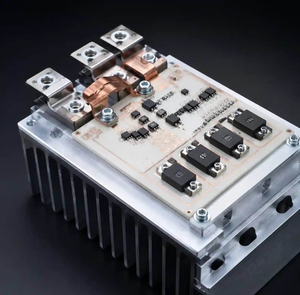
Ceramic substrates provide excellent in-plane thermal conductivity, but you must design thermal paths from heat sources to heat sinks. Design considerations include:
- Place high-power components near board edges for heat sink attachment
- Minimize thermal resistance between component and ceramic substrate
- Use thermal vias in multilayer LTCC for vertical heat extraction
- Account for thermal interface materials (TIM) in junction-to-case calculations
CTE Matching Considerations
Coefficient of thermal expansion mismatch creates mechanical stress during temperature cycling. CTE values for reference:
- Silicon semiconductors: 2.6-3.5 ppm/°C
- AlN ceramic: 4.5-5.7 ppm/°C (excellent match)
- Al₂O₃ ceramic: 6.5-7.2 ppm/°C (acceptable match)
- Copper: 17 ppm/°C (significant mismatch)
You should evaluate thermal cycling requirements and select substrate materials with CTE values closest to your semiconductor devices for applications experiencing -40°C to +150°C or wider temperature ranges.
FAQs
What is the main difference between DBC and AMB ceramic PCB processes?
DBC (Direct Bonded Copper) uses eutectic oxidation bonding at 1065-1083°C and works exclusively with alumina (Al₂O₃) substrates. AMB (Active Metal Brazing) uses brazing alloys containing titanium at 800-900°C and bonds to aluminum nitride (AlN) and silicon nitride (Si₃N₄) ceramics that DBC cannot process. AMB with AlN substrates achieves 150-230 W/mK thermal conductivity compared to DBC alumina at 24-28 W/mK, but costs 3-5× more.
When should I choose LTCC instead of DBC or AMB?
Choose LTCC when you need complex multilayer RF circuits with 8+ layers, embedded passive components (resistors, capacitors, inductors), hermetic packaging for harsh environments, or three-dimensional integration that planar DBC/AMB cannot achieve. LTCC excels in wireless communication modules, automotive radar systems, and miniaturized medical devices where circuit complexity outweighs maximum thermal conductivity requirements.
What copper thickness should I specify for ceramic PCB power modules?
For power electronics applications, specify 0.3mm (300μm) copper for 50-150A current handling, 0.4mm for 150-300A, and 0.6-0.8mm for extreme current requirements above 300A. Calculate based on 1-3 A/mm² current density for continuous operation. Standard DBC and AMB processes support 0.2-0.8mm copper thickness—significantly thicker than conventional PCB assembly copper layers.
Can ceramic PCBs be manufactured with multiple layers like standard PCBs?
DBC and AMB technologies are primarily single or double-sided processes—copper bonded to one or both sides of a ceramic substrate. LTCC technology creates true multilayer structures with 2-50+ layers by stacking and co-firing ceramic tapes. For multilayer high-power designs, you can combine ceramic substrates with standard rigid flex PCB assemblies or specify LTCC if thermal requirements (3-5 W/mK) are adequate.
What is the typical lead time for ceramic PCB manufacturing?
DBC alumina substrates typically require 2-4 weeks lead time for standard designs. AMB substrates with AlN or Si₃N₄ ceramics need 3-6 weeks due to specialized brazing processes and material procurement. LTCC manufacturing takes 4-8 weeks due to multilayer processing complexity, tape preparation, and firing schedules. You should plan longer development timelines for ceramic substrates compared to quick turn PCB assembly of standard FR-4 boards.
How do I calculate which ceramic process my application needs?
Calculate total power dissipation, component junction temperature limits, and thermal resistance requirements from junction to ambient. If thermal analysis shows alumina (24-28 W/mK) maintains components within temperature limits, specify cost-effective DBC. If calculations require >50 W/mK thermal conductivity or severe thermal cycling demands better CTE matching, specify AMB with AlN substrates. For RF circuits requiring multilayer integration beyond planar capability, specify LTCC regardless of thermal conductivity.
Conclusion
Ceramic PCB manufacturing encompasses three primary processes—DBC, AMB, and LTCC—each optimized for distinct application requirements in power electronics, RF systems, and high-reliability devices. DBC technology bonds copper to alumina substrates at 1065-1083°C, providing cost-effective thermal management (24-28 W/mK) for automotive, solar, and industrial power electronics. AMB uses active metal brazing to bond copper to aluminum nitride and silicon nitride ceramics, achieving superior thermal conductivity (150-230 W/mK) and CTE matching essential for high-power electric vehicle inverters, SiC/GaN modules, and aerospace applications. LTCC co-fires multilayer ceramic structures at 850-900°C, enabling complex RF circuits with embedded passives for wireless communication, automotive radar, and miniaturized medical devices.
Your process selection should be based on quantitative thermal analysis, substrate material requirements, circuit complexity, and cost constraints. Specify DBC for alumina-based power electronics where 24-28 W/mK thermal conductivity is adequate and cost-effectiveness is critical. Choose AMB when maximum thermal performance, superior CTE matching, or nitride ceramic properties justify 3-5× higher cost. Select LTCC when multilayer RF integration and embedded passives outweigh the thermal conductivity limitations compared to DBC and AMB technologies.
If you need high-quality ceramic PCB manufacturing for your power electronics or RF project, Andwin Circuits offers advanced DBC and AMB ceramic substrate capabilities with thermal management expertise. Our manufacturing facility provides metal core PCB and special PCB solutions for automotive, LED lighting, telecommunications, and industrial applications. We are certified to ISO 9001, IATF 16949, and UL standards, ensuring superior quality for high-reliability electronics worldwide.
Contact us today for ceramic substrate design consultation, thermal analysis support, and competitive factory-direct pricing tailored to your specific application requirements.