
Skip to content
Andwin Circuits
  • Home
  • ProductsExpand
    • HDI multilayer PCB
    • Rigid Flex PCB
    • Flex pcb
    • Special PCBExpand
      • High Frequency PCBExpand
        • Rogers RO4350B PCB
        • Rogers RO4003 pcb
        • Rogers RO3003 PCB
        • Rogers 5880 PCB
        • DICLAD 527 PCB
        • Taconic TLX series
        • Taconic TLX-8 RF PCB
        • Taconic TLX-9 RF PCB
      • High speed pcbExpand
        • Megtron 6 High Speed PCB
        • TU-872 SLK Sp High Speed
      • High TG PCBExpand
        • SHENGYI SH260 PCB
        • ISOLA 370HR PCB
        • ISOLA IS410 PCB
        • ISOLA IS420 PCB
      • Heavy copper PCB
      • Copper coin pcb
      • Copper inlay PCB
    • Metal Core PCBExpand
      • Copper core pcb
      • Aluminum PCB
      • 2 Layers Aluminum PCB
      • Direct thermal MCPCB
      • 2 Layers Direct Thermal
    • Ceramic PCBExpand
      • DPC ceramic PCB
      • DBC ceramic PCB
      • Thick film Ceramic PCB
      • Al2O3 Alumina PCB
      • AIN ALN ceramic PCB
      • IGBT Ceramic PCB
  • ServiceExpand
    • PCB Assembly
    • Quick turn PCB assembly
    • PCBA conformal coating
  • IndustryExpand
    • Telecommunication
    • IoT and Wireless
    • Industrial Control
    • Thermal management
    • Power and Energy
    • IC test board
    • Automative
    • Medical
  • CapabilityExpand
    • Rigid PCB
    • Rigid flex PCB
    • Metal core PCB
    • PCB Assembly
  • TechnologyExpand
    • Blogs
    • Via in pad
    • PCB E-test
    • PCB stack up
    • MCPCB panelization
    • Controlled impedance PCB
  • AboutExpand
    • About us
    • Certification
    • Factory Tour
  • Contact
Andwin Circuits
Home / Determination of Creepage and Clearance in PCB Layout

Determination of Creepage and Clearance in PCB Layout

ByGrace June 3, 2025May 30, 2025

1. Introduction

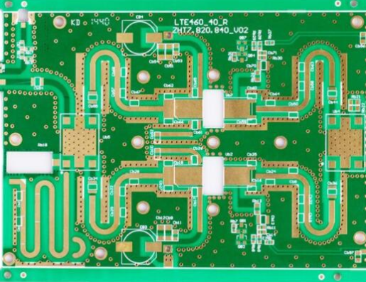
Printed Circuit Board (PCB) design involves numerous critical considerations to ensure reliability, safety, and compliance with industry standards. Among these, creepage distance and clearance (electrical gap) are fundamental parameters that influence the PCB’s performance, especially in high-voltage and high-reliability applications.

Improper spacing between conductive elements can lead to electrical breakdown, arcing, or short circuits, compromising the board’s functionality and safety. This article explores the definitions, determining factors, calculation methods, and design best practices for creepage and clearance in PCB layout.
Contact us for PCB quote now |

2. Definitions: Creepage vs. Clearance

2.1 Clearance (Electrical Gap)

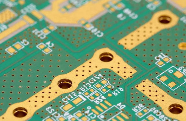
Clearance refers to the shortest distance in air between two conductive parts. It determines the minimum air gap required to prevent dielectric breakdown or arcing due to high voltage differences.

  • Key Influencing Factors:
  • Voltage difference between conductors
  • Altitude (air density affects dielectric strength)
  • Pollution degree (conductive dust, moisture)
  • Transient overvoltages (surges, spikes)

2.2 Creepage Distance

Creepage is the shortest path along the surface of an insulating material between two conductive parts. It prevents tracking, where conductive paths form due to contamination or moisture.

  • Key Influencing Factors:
  • Voltage difference
  • Pollution degree (dust, humidity)
  • Material Comparative Tracking Index (CTI)
  • Environmental conditions (indoor vs. outdoor)
Contact us for PCB quote now |

3. Standards and Regulations

Several international standards define minimum creepage and clearance requirements:

  • IEC 60664-1 – Insulation coordination for low-voltage equipment
  • IPC-2221 – Generic standard for PCB design
  • UL 60950-1 / IEC 62368-1 – Safety requirements for IT equipment
  • IEC 61010-1 – Safety for laboratory and measurement equipment

These standards classify pollution degrees (1 to 4) and material groups (I to IIIa) based on CTI values.

4. Calculating Creepage and Clearance

4.1 Clearance Calculation

The required clearance depends on:

  • Working voltage (AC/DC)
  • Altitude (higher altitudes require larger clearances due to reduced air density)
  • Pollution degree (more contamination increases risk of arcing)

Example (per IPC-2221):

  • For 100V DC, Pollution Degree 2, the minimum clearance is 0.1 mm.
  • For 250V AC, Pollution Degree 3, the minimum clearance increases to 1.5 mm.

4.2 Creepage Calculation

Creepage depends on:

  • Voltage
  • Pollution degree
  • Material group (CTI value)

Example (IEC 60664-1):

  • For Material Group IIIa (CTI ≥ 600), 250V AC, Pollution Degree 2, the minimum creepage is 1.5 mm.
  • For Material Group II (CTI 400-599), the same conditions require 2.0 mm.
Contact us for PCB quote now |

5. Design Best Practices

5.1 Increasing Creepage Distance

  • Slotting PCBs – Adding milled slots increases surface distance.
  • Using Conformal Coating – Protects against moisture and contamination.
  • Selecting High-CTI Materials – FR4 with high CTI (>600) improves tracking resistance.

5.2 Optimizing Clearance

  • Avoid Sharp Edges – Rounded pads reduce corona discharge.
  • Use High-Voltage Components – Select parts rated for higher voltages.
  • Consider Altitude Effects – Derate clearance for high-altitude applications.

5.3 Software Tools

Modern PCB design tools (Altium, KiCad, Cadence) include Design Rule Checks (DRC) to verify creepage and clearance compliance.

6. Common Mistakes and Mitigations

  • Ignoring Pollution Degree – Assume worst-case environmental conditions.
  • Insufficient Margin for Transients – Account for voltage spikes.
  • Poor Material Selection – Low-CTI materials increase tracking risk.

7. Conclusion

Proper determination of creepage and clearance is essential for safety, reliability, and compliance in PCB design. By following industry standards, selecting appropriate materials, and applying best practices, engineers can mitigate risks of electrical breakdown and ensure long-term performance.

Future advancements in high-voltage PCB materials and automated DRC tools will further enhance design precision, making adherence to creepage and clearance requirements more efficient.

Contact us for PCB quote now |
Post Tags: #aluminum clad pcb#aluminum core pcb#aluminum pcb#assemble pcb#PCB layout

Post navigation

Previous Previous
Handling Inductors in PCB Design: Techniques and Best Practices
NextContinue
Why PCB Impedance Can Be Controlled: A Comprehensive Analysis

Search

Search

Products

  • HDI Multilayer PCB
  • Rigid Flex PCB
  • Flex pcb
  • High Frequency PCB
  • High speed pcb
  • Heavy copper PCB
  • Metal Core PCB
  • Ceramic PCB

Address

Andwin Circuits Co.,Limited
Email: sales@andwinpcb.com
Tel: +86 755 2832 9394
Fax:+86 755 2992  6717
ADD:1-2F-1217,HouDeQun Industrial park,
NanTing RD NO.56,ShaJing,BaoAn,Shenzhen 518104,GuangDong,China

Products

  • HDI Multilayer PCB
  • Rigid Flex PCB
  • Flex pcb
  • High Frequency PCB
  • High speed pcb
  • Heavy copper PCB
  • Metal Core PCB
  • Ceramic PCB

Technology

  • Blogs
  • Via in pad
  • PCB E-test
  • PCB stack up
  • Metal core PCB panelization
  • Controlled impedance PCB

CERTIFICATION

Certification >>


Copyright© 2003 - 2026 Andwin | All Rights Reserved | Powered by Andwin

Scroll to top
  • Home
  • Products
    • HDI multilayer PCB
    • Rigid Flex PCB
    • Flex pcb
    • Special PCB
      • High Frequency PCB
        • Rogers RO4350B PCB
        • Rogers RO4003 pcb
        • Rogers RO3003 PCB
        • Rogers 5880 PCB
        • DICLAD 527 PCB
        • Taconic TLX series
        • Taconic TLX-8 RF PCB
        • Taconic TLX-9 RF PCB
      • High speed pcb
        • Megtron 6 High Speed PCB
        • TU-872 SLK Sp High Speed
      • High TG PCB
        • SHENGYI SH260 PCB
        • ISOLA 370HR PCB
        • ISOLA IS410 PCB
        • ISOLA IS420 PCB
      • Heavy copper PCB
      • Copper coin pcb
      • Copper inlay PCB
    • Metal Core PCB
      • Copper core pcb
      • Aluminum PCB
      • 2 Layers Aluminum PCB
      • Direct thermal MCPCB
      • 2 Layers Direct Thermal
    • Ceramic PCB
      • DPC ceramic PCB
      • DBC ceramic PCB
      • Thick film Ceramic PCB
      • Al2O3 Alumina PCB
      • AIN ALN ceramic PCB
      • IGBT Ceramic PCB
  • Service
    • PCB Assembly
    • Quick turn PCB assembly
    • PCBA conformal coating
  • Industry
    • Telecommunication
    • IoT and Wireless
    • Industrial Control
    • Thermal management
    • Power and Energy
    • IC test board
    • Automative
    • Medical
  • Capability
    • Rigid PCB
    • Rigid flex PCB
    • Metal core PCB
    • PCB Assembly
  • Technology
    • Blogs
    • Via in pad
    • PCB E-test
    • PCB stack up
    • MCPCB panelization
    • Controlled impedance PCB
  • About
    • About us
    • Certification
    • Factory Tour
  • Contact
Search