
Handling Inductors in PCB Design: Techniques and Best Practices
Introduction
Printed Circuit Board (PCB) design is a complex process that involves careful consideration of various electronic components, including resistors, capacitors, and inductors. Among these, inductors are particularly challenging due to their inherent electromagnetic properties, which can significantly impact circuit performance if not properly managed.
Inductors are passive components that store energy in a magnetic field when electric current flows through them. They are widely used in power supplies, RF circuits, filters, and signal conditioning applications. However, their behavior can introduce parasitic effects, electromagnetic interference (EMI), and unwanted coupling if not handled correctly in PCB layouts.
This article explores key techniques for managing inductors in PCB design, covering inductor selection, placement, routing, grounding, and EMI mitigation strategies.
1. Understanding Inductor Characteristics in PCB Design
Before implementing inductors in a PCB, designers must understand their key characteristics:
- Self-Resonant Frequency (SRF): Every inductor has a frequency at which it behaves like a resonant circuit due to parasitic capacitance. Beyond this frequency, the inductor loses its inductive properties.
- DC Resistance (DCR): The inherent resistance of the inductor’s wire, which causes power loss and heating.
- Saturation Current: The maximum current an inductor can handle before its magnetic core saturates, reducing inductance.
- Parasitic Effects: Stray capacitance and mutual inductance can affect signal integrity.
These factors must be considered when selecting and placing inductors on a PCB.
2. Inductor Selection for PCB Applications
Choosing the right inductor is critical for optimal performance. Key considerations include:
2.1. Inductor Types
- Wirewound Inductors: High inductance but larger size; suitable for power applications.
- Multilayer Ceramic Inductors: Compact and ideal for high-frequency circuits.
- Ferrite Core Inductors: Provide high inductance with low losses but can saturate at high currents.
- Shielded vs. Unshielded Inductors: Shielded inductors reduce EMI but may have higher DCR.
2.2. Key Parameters
- Inductance Value: Must match the circuit requirements.
- Current Rating: Should exceed the maximum expected current to avoid saturation.
- Q Factor (Quality Factor): Higher Q indicates lower energy loss.
- Temperature Stability: Important for high-power or high-frequency applications.
3. PCB Layout Techniques for Inductors
Proper placement and routing of inductors are crucial to minimize noise and interference.
3.1. Placement Strategies
- Keep Inductors Away from Sensitive Components: High-current inductors can generate magnetic fields that interfere with nearby traces or ICs.
- Minimize Loop Areas: Reduce parasitic inductance by keeping current loops small.
- Orientation Matters: Place inductors perpendicular to each other to minimize mutual coupling.
3.2. Routing Considerations
- Use Short and Wide Traces: Reduces parasitic resistance and inductance.
- Avoid Sharp Corners: 90-degree bends increase parasitic effects; use 45-degree angles instead.
- Separate High-Frequency and Low-Frequency Paths: Prevents crosstalk.
3.3. Grounding Techniques
- Use a Solid Ground Plane: Provides a low-impedance return path.
- Avoid Ground Loops: Ensure a single-point ground for high-frequency circuits.
- Star Grounding for Mixed-Signal Designs: Separates analog and digital grounds to reduce noise.
4. Mitigating EMI and Noise
Inductors can be sources of electromagnetic interference (EMI). Effective strategies include:
4.1. Shielding Techniques
- Use Shielded Inductors: Contain magnetic flux within the component.
- Ferrite Beads: Suppress high-frequency noise in power and signal lines.
- Ground Shields: Metal shielding around inductors can reduce radiated emissions.
4.2. Decoupling and Filtering
- Place Decoupling Capacitors Near Inductors: Stabilizes voltage and reduces high-frequency noise.
- LC Filters: Used to suppress unwanted oscillations and harmonics.
4.3. Proper Return Paths
- Ensure Low-Impedance Return Paths: Reduces ground bounce and EMI.
- Avoid Splitting Ground Planes Under Inductors: Prevents unwanted inductance in return paths.
5. Thermal Management
Inductors, especially in power applications, can generate significant heat. Proper thermal design includes:
- Adequate Copper Pouring: Helps dissipate heat.
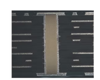
- Thermal Vias: Used to transfer heat to inner or bottom layers.
- Avoid Overcrowding: Ensures proper airflow and cooling.
6. Simulation and Testing
Before finalizing the PCB, simulations and tests should be performed:
- SPICE Simulations: Analyze inductor behavior in the circuit.
- Impedance Analysis: Ensures the inductor operates as intended.
- EMI Testing: Validates noise suppression techniques.
Conclusion
Inductors play a vital role in PCB design but require careful handling to avoid performance issues. By selecting the right inductor type, optimizing placement and routing, implementing proper grounding, and mitigating EMI, designers can ensure reliable and efficient circuit operation. Thermal management and thorough testing further enhance design robustness.
Following these best practices will help PCB designers effectively integrate inductors while minimizing unwanted effects, leading to higher-quality electronic products.