
Development Trends of Foreign Printed Circuit Board Manufacturing Technology
I. Brief Introduction to Foreign Printed Circuit Board Manufacturing Technology
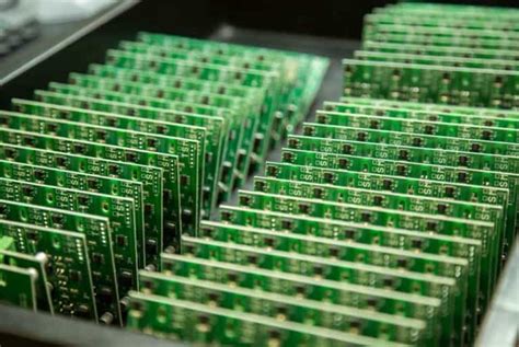
With the development of micro-device manufacturing and surface mounting technology, the manufacturing technology of printed circuit boards has been innovated and improved faster, especially the wire width of circuit graphics. Currently, the widely used wire width abroad is three wires between pins, and the wire width that reaches the practical stage is 4-5 wires between pins, and it is developing towards a thinner wire width. In order to adapt to the narrow spacing of SMD multi-leads, the wiring of printed circuit boards is thinned. The popularized processes are: the CAD/CAM system is widely used, and the data provided by the design is converted into production data through the manufacturing system; thin copper foil and thin dry film photoresist are used in raw materials; due to the narrow pitch, the printed circuit board surface requires a smooth and flat copper surface to make micro pads and circuit patterns with fine lines and narrow pitches; the substrate used should have a high thermal shock resistance, so that the printed circuit board will not produce defects such as bubbles, delamination and pad bulging during the electrical installation process, ensuring the high reliability of surface mounted components; and high-viscosity copper foil and modified epoxy resin are used to ensure that they maintain sufficient bonding strength at the welding temperature, and should also have high dimensional stability to ensure the consistency and accuracy of the positioning of fine circuit patterns during the production process. In short, the manufacturing technology of printed circuit boards with fine wires and narrow pitches is developing very fast. If you want to keep up with the world’s advanced technology level, you must understand the current development trends in this area abroad.
2.Development trends of key process technologies abroad
(1)Film production and pattern transfer process
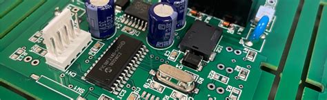
The quality of film production and pattern transfer directly affects the quality of fine circuit patterns. Therefore, when making negatives, computer-aided design systems (CAD) are generally used to design circuits and interface with computer-aided manufacturing systems (CAM) to produce high-precision, high-resolution photo-drawing negatives through data conversion. Due to the high density of wires, the wire width and spacing are 0.10-0.05mm. In order to ensure the precision and accuracy of the negative wire graphics and the quality of circuit graphics imaging, the cleanliness of the workroom is required to be high, usually using Class 10,000 or Class 1,000 to ensure the high quality of film imaging.
In terms of graphic transfer technology, the materials used for imaging are thin photosensitive resists with high resolution, CD (electrophoresis) and liquid photosensitive solder resists for soldering. Among them, the photoresist layer coated by electrophoresis has a thickness of 5-30 microns and is controllable, with a resolution of 0.05-0.03mm. It plays a great role in improving the accuracy and consistency of fine circuit graphics and solder resist graphics.
In the process of circuit graphics transfer, in addition to strictly controlling the process parameters, the cleanliness of the workroom is also very high, reaching the Class 10,000 standard or less. In order to ensure the high quality of graphic transfer, it is also necessary to ensure the indoor working conditions, such as controlling the indoor temperature at 21±1℃ and the relative humidity at 55-60%. The negatives and semi-finished products of graphic transfer imaging must be inspected 100%.
(2)Drilling process technology
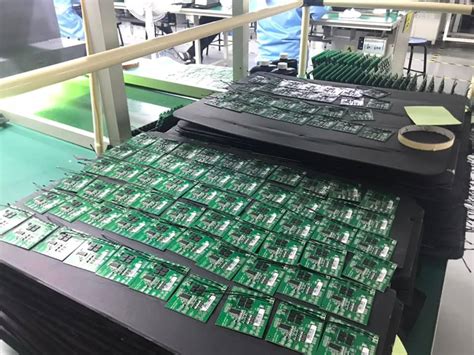
The drilling quality must first ensure the high reliability and high quality of the electroplated through-holes, so the drilling quality must be strictly controlled. Both at home and abroad attach great importance to this aspect. In particular, the thickness and aperture of the surface mounted multilayer printed circuit board are relatively high, so the quality of the electroplated through-hole has become the key to improving the qualified rate of the surface mounted printed circuit board. At present, foreign countries use a diameter of 0.25-0.30mm in the selection of through-hole aperture size. The key to the miniaturization of through-holes is the development and use of high-precision and high-stability CNC drilling machines. In recent years, foreign countries have developed and used CNC drilling machines and special tools that can drill holes with a diameter of 0.10mm. In terms of drilling, experience tells us that it is very important to correctly select drilling process parameters based on the study of the physical and chemical properties of the substrate. At the same time, the auxiliary materials and matching fixtures (such as upper and lower pads, positioning methods, drill bits, etc.) should be correctly selected. Laser drilling technology is also used to adapt to micro-apertures.
(3)Hole metallization technology
In terms of hole metallization technology, in order to ensure the high reliability of hole metallization quality, a new type of pitting and decontamination process, namely the low-alkaline potassium permanganate method, is used in the pretreatment after drilling to provide a very excellent hole wall surface and eliminate wedge grooves and crack defects. And adopt advanced direct electroplating process, vacuum metallization process and other process methods to meet the metallization needs of small holes, micro holes, blind holes and buried holes of various types of printed circuit boards.
(4)Vacuum lamination process
Especially for the manufacture of multi-layer pressed printed circuit boards, vacuum multi-layer presses are widely used abroad. This is because the internal graphics of surface mounted multi-layer printed circuit boards have characteristic impedance (Z0) requirements. Because the characteristic impedance is related to the thickness of the dielectric layer and the width of the conductor (see the following formula):
Z0=60 /ε.LN .4H/D0&n bsp; Note: ε is the dielectric constant of the material
H is the thickness of the dielectric material
D0 is the actual width of the conductor
The dielectric constant and the actual width of the conductor are known, so the thickness of the dielectric material becomes the key factor of the characteristic impedance. The use of vacuum lamination equipment and computer control has significantly improved the lamination quality. Because the layers of the multi-layer printed circuit board have been vacuum-exhausted before vacuum lamination to remove low-molecular volatiles, the lamination pressure is significantly reduced, which is only 1/4-1/2 of the lamination pressure of the conventional multi-layer printed circuit board, so that the thickness of the dielectric material between the conductor pattern layers of the multi-layer printed circuit board is uniform, with high precision and small tolerance, ensuring the technical indicators of the characteristic impedance Z0 within the design requirements. At the same time, the use of vacuum lamination technology can improve the surface flatness of the multi-layer printed circuit board and reduce the quality defects of the multi-layer printed circuit board (such as lack of glue, delamination, white spots and dislocation, etc.).
3.Detection technology is an important means to ensure the implementation of the process
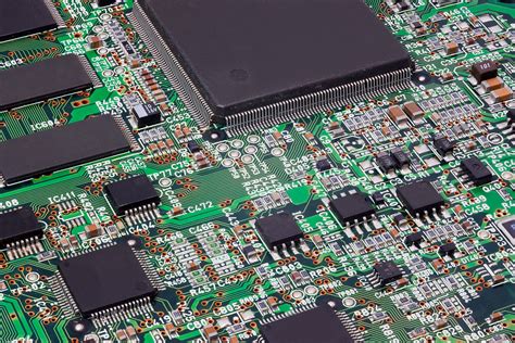
According to the development of electrical technology from pin insertion technology to surface packaging technology (bare chip direct installation technology and fine pitch technology) – multi-chip module (MCM) technology or multi-chip packaging technology, the detection of circuit graphics of multi-layer printed circuit boards has become more difficult. For this reason, both at home and abroad are developing and using high-precision and high-stability detection equipment. At present, there are two types of detection equipment, namely non-contact and contact.
(1)Non-contact detection technology
Detection technology is an important means to provide physical and chemical performance data of printed circuit boards. With the changes in the accuracy and density of printed graphics, the use of artificial visual methods for a long time in the past has not been able to meet the needs of high-tech development. Detection technology and equipment have developed rapidly, gradually replacing manual visual inspection to judge product quality in terms of use function. It has moved from the appearance detection of circuit graphics to the detection of inner circuit graphics, thereby pushing simple detection to the direction of combining quality monitoring between processes and defect repair. Its main features are: the use and application of computer software and hardware technology, high-speed image processing and pattern recognition technology, high-speed processing hardware, automatic control, precision machinery and optical technology, and it is a product of a variety of high technologies. It does not touch, destroy or damage the inspection components, and can inspect places that cannot be inspected by contact. The equipment includes the following:
Bare board appearance inspection technology and equipment
That is, AOI (optical tester). It mainly uses the design specification inspection method to test two-dimensional digital graphics. With the emergence of surface mounting technology and three-dimensional molded printed circuit boards, the design specification inspection method will have completely different connotations. It can not only detect the width of wires and line spacing, but also the height of wires. Therefore, the existence of three-dimensional layout must be more advanced sensors and imaging technology. Non-contact AOI testing technology is a product that integrates X-rays, infrared technology, and other inspection technologies.
X-ray inner layer perspective inspection technology
The X-ray used in the early days had a focal length as large as 300μm, and its detection accuracy could only reach 0.05mm. At present, the focal length has reached the micron level, and it can be measured with an accuracy of 10 microns. Used in conjunction with image processing, it can perform high-resolution perspective and inspection of the inner layer circuit graphics of multi-layer printed circuit boards.
(2)Contact detection technology and equipment
The detection method for printed circuit boards mainly uses online testers, also known as static functional tests. There are many models at present, and advanced equipment can quickly detect quality defects (including open circuits and short circuits) caused by errors in the manufacturing process. There are general-purpose on-off testers, special on-off testers, and flying probe mobile on-off testers. The latter is suitable for small batches of high-density, high-precision double-sided and multi-layer printed circuit boards.
Article address: https://www.eechina.com/thread-27131-1-1.html [Print this page]
Some articles on this site are reprinted or posted by netizens for the purpose of conveying and sharing information, and do not mean that this website agrees with its views and is responsible for its authenticity; the copyright of the article belongs to the original author and the original source. If it involves the content of the work, copyright and other issues, we will correct or delete it as soon as possible according to the requirements of the copyright owner.