
Eco-Friendly PCB Design Tips: Reduce Electronic Waste
As PCB designers, we have a role to play in reducing the environmental and health impacts of electronic waste. To do this, we need to figure out the materials used in our designs, their impact on the planet, and how to optimize our designs to reduce electronic waste.
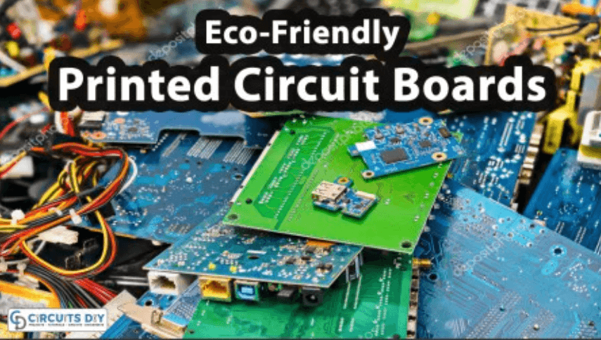
Why is electronic waste dangerous?
From the latest smartphone to the bulky 40-inch TV, every PCB that ends up in a landfill is harmful to the environment. You may love the PCBs and components of your latest prototype, but they are made from chemicals that can cause a variety of health issues.
Both cadmium and beryllium are present in electronic parts. They are known to cause cancer in humans. Electronics may also contain mercury, which can be highly toxic even in the shortest of times. A more familiar name may be lead, which is extremely toxic, especially to young children.
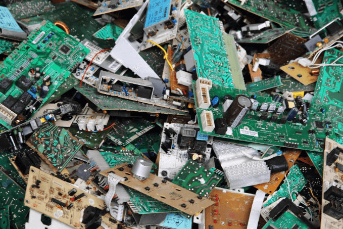
Discarded electronic devices are discarded and fill up landfills, which means these chemicals leak into the environment. It can cause serious pollution to nearby rivers or air simply by releasing toxic particles into the surrounding environment.
Can electronic waste be recycled?
To a certain extent, electronic waste can be recycled. Gold, copper, and aluminum found in electronics are precious materials that can be reused. However, recycling electronic waste is not a simple process.
Sorting, cleaning, and size reduction involve complex processes before separating useful materials from non-reusable materials. Since electronics contain hazardous chemicals, strict safety precautions must be taken during the recycling process.
Recycling of electronic waste is an expensive affair. It only makes sense if the cost of recovering precious metals such as gold is lower than the cost of mining them from the earth. Recycling will reduce the impact of electronic waste on the earth by properly handling toxic residues, but it is not a perfect solution.
How to Reduce Electronic Waste in PCB Design
With Restriction of Hazardous Substances (RoHS) compliance, restricted hazardous materials should be avoided in the design. One place to start with reducing electronic waste is to adhere to and pay careful attention to RoHS compliance. RoHS regulations are designed to restrict or eliminate substances that are harmful to the environment and humans.
You can add RoHS compliance, WEEE compliance, or the Waste Electrical and Electronic Equipment Directive, which are responsible for the proper handling of much of the same equipment that RoHS regulates.
Like it or not, there are still electronics that end up in landfills, even with recycling facilities available. As a PCB designer, you can play your part in minimizing the impact of e-waste on the environment.
Biodegradable PCBs
At the time of writing, biodegradable PCBs are not yet a reality, but researchers have made progress toward them. A team of researchers has managed to replace conventional metal conductors in PCBs with transient metal pastes made of zinc and tungsten.
These transient metals gradually dissolve when immersed in water. While more research needs to be done, the demonstration of water-soluble PCBs is promising progress at a time when the threat of e-waste to the environment is growing.
Design for serviceability
It would be foolish to assume that every PCB deployed will last a decade or so. There are bound to be defects, damage due to wear and tear or electrical transients. In such cases, PCBs designed for serviceability increase the likelihood of making it to a repair rather than landfill.
Design for serviceability involves a variety of considerations. For example, you need to ensure that components are properly labeled so that technicians can easily find and correct faults. This also means dispensing surge suppression components if the PCB is used in an outdoor environment.
Modular Design
Understandably, consumer products are pushing for smaller sizes. However, when you are involved in commercial or industrial applications where size is not a critical factor, consider a modular approach in PCB design.
Instead of a single PCB, it makes sense to divide the design into several or more parts. For example, microcontrollers and other SMD ICs are placed on one PCB, and wire-to-board connectors are on another.
With this approach, upgrading the MCU or SMD IC would only result in replacing half of the total PCB size. PCB modular design involves precise dimensions to ensure accurate connection of multiple PCBs, especially when built in a stackable manner.