
Electromagnetic compatibility analysis of multi-layer PCB boards PCB proofing
Electromagnetic compatibility analysis of multi-layer PCB boards can be based on Kirchhoff’s law and Faraday’s law of electromagnetic induction.
Based on the above two laws, we conclude that the following basic principles should be followed by the layering and stacking of multi-layer printed circuit boards:
1 The power plane should be as close to the ground plane as possible and should be lower than the ground plane.
2 The wiring layer should be adjacent to the image plane layer.
3 The power supply and ground layer impedance are the lowest. Where the power supply impedance Z0 = Where D is the distance between the power plane and the ground plane. W is the area between the planes.
4 A stripline is formed in the middle layer and a microstrip line is formed on the surface. The characteristics of the two are different.
5 Important signal lines should be close to the ground.
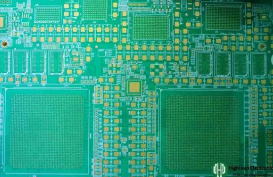
Stacking and layering PCB boards
1 Double-layer board. This circuit board can only be used for low-speed design. EMC is relatively poor.
2 Four-layer board. The stacking order is as follows. Different stacking advantages and disadvantages are explained below.
The case should be the best case for a four-layer board. Since the outer layer is the ground layer, it has a shielding effect on EMI, and the power layer is close to the ground layer, which is also reliable, so the internal resistance of the power supply is small, and the best suburban fruit can be obtained. However, when the density of the circuit board is relatively large, the first case cannot be used. Therefore, the integrity of the first layer cannot be guaranteed, and the second layer signal will become worse. In addition, this structure cannot be used when the power consumption of the whole board is relatively large.
Case B is the most common way we usually use. From the structure of the circuit board, it is not suitable for high-speed digital circuit design. Because in this configuration, it is difficult to maintain low power supply impedance. Take a 2 mm board as an example: Z0 = 50 ohms is required. The line width is 8 mils. The thickness of the copper foil is 35μm. Therefore, the middle of the signal layer between the ground and the ground is 0.14mm. Form and power layer is 1.58mm. This greatly increases the internal resistance of the power supply. In this structure, since the radiation is spatial, a shielding board needs to be added to reduce EMI.
In the case of C, the signal quality of the S1 layer is the best. S2 ranks second. It has a shielding effect on EMI. However, the power supply impedance is large. This circuit board can be used when the power consumption of the entire circuit board is large and the circuit board is an interference source or close to an interference source.
3 Six-layer circuit board
Case is one of the common methods, S1 is a good wiring layer. S2 ranks second. However, the power plane impedance is poor. Pay attention to the influence of S2 on the S3 layer when routing.
In case B, the S2 layer is a good wiring layer of the S3 level. The power plane impedance is better.
For C, this is the best case for a six-layer circuit board, S1, S2, and S3 are all good wiring layers. The power plane impedance is better. The fly in the ointment is that the wiring layer is one layer less than the first two cases.
In case D, in the six-layer board, although the performance is better than the first three, the wiring layer is less than the first two. This situation is mainly used on the backplane.
4 Eight-layer board
Eight-layer board, if there are 6 signal layers, it is best to use A. However, this arrangement is not suitable for high-speed digital circuit design. If it is 5 signal layers, it is best to use C. In this case, S1, S2, and S3 are all good wiring layers. At the same time, the power plane impedance is also relatively low. If it is 4 signal layers, it is best to use B in Table 3. Each signal layer is a good wiring layer. In these cases, adjacent signal layers should be routed.
5 ten-layer boards
If there are 6 signal layers in the ten-layer board, there are three stacking sequences A, B and C. Case A is the best, C type is the second, and case B is the worst. Other cases not listed are worse than these cases. In case A, S1, S6 are better wiring layers. S2, S3, S5 second. It should be pointed out in particular that the reason why A is better than C is the same as C. The main reason is that in case C, the distance between the GND layer and the POWER layer is determined by the distance between S5 and GND. This does not necessarily ensure that the GND layer and the POWER layer have the lowest power plane impedance. Case D should be said to be the best stacking sequence of ten layers. Each signal layer is an excellent wiring layer. E and F are mainly used for rebounding. Among them, the shielding effect of F is better than that of E. The disadvantage is that the two signal layers are connected, and attention should be paid to routing.
In short, the layering and lamination of PCB is a complex issue. There are many factors to consider. But we should keep in mind the functions we want to accomplish and the key factors required. In this way, we can find the layering and laminating printing board sequence that meets our requirements.