
HDI PCB Any Layer Interconnection: mSAP Process Advantages for High-Density Design (2026)
Want to route 25μm traces between 0.4mm pitch BGA pads? That’s where mSAP comes in. Traditional subtractive PCB fabrication hits a wall around 50-75μm—any finer and the etch undercut eats your traces. The modified Semi-Additive Process builds copper instead of etching it away, giving you near-vertical sidewalls and 25/25μm line/space. For engineers working on advanced HDI designs, partnering with a PCB manufacturer that has proven mSAP capability is essential to achieving these fine geometries at production yields. Here’s what engineers need to know to make it work.
What is Any Layer Interconnection?
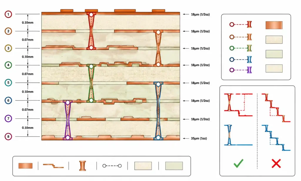
Any Layer HDI lets you connect between non-adjacent layers through stacked or staggered microvias—not just layer-to-layer like 1+N+1 or 2+N+2 structures. That means fewer vias, shorter signal paths, and better signal integrity for complex, high-pin-count designs like mobile processors, AI accelerators, and advanced comms modules.
But the catch: you need small, reliable microvias with consistent aspect ratios and fine trace geometries. Traditional subtractive processing can’t reliably produce traces below 50μm with acceptable tolerances. mSAP solves that by building traces additively, enabling 25/25μm line/space—the same kind of ultra-fine geometry covered in our FPC minimum line width/spacing guide, which dives deeper into 0.05mm trace rules and their impact on yield.
The mSAP Process Explained
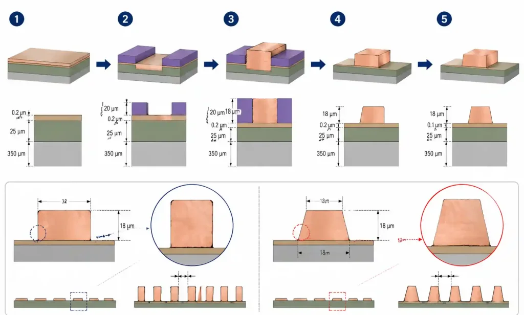
Subtractive processes start with a full copper layer, then etch away what you don’t want. This gives you trapezoidal trace profiles because the etchant undercuts the resist. mSAP reverses this: start with a thin seed layer (0.5-1.0μm), apply resist, electroplate copper only where you need traces, strip the resist, and flash-etch the seed layer. Since you’re only removing a thin seed layer, undercut is minimal and you get near-vertical sidewalls.
Key process steps:
- Substrate prep with roughness treatment for adhesion
- Sputtering or electroless copper deposition for uniform seed layer
- Dry film resist lamination and LDI exposure for pattern definition
- Copper electroplating to build trace thickness (10-15μm typical)
- Resist stripping and flash etching of the seed layer
The result: dimensional accuracy within ±5μm for line width and spacing, compared to ±15-25μm typical of subtractive processes.
Key Advantages for HDI Design
Routing density: 25/25μm or 30/30μm geometries give you 30-50% more routing density. Route 3-4 traces between 0.4mm pitch BGA balls versus only 2 with subtractive methods. Often eliminates one or two signal layers.
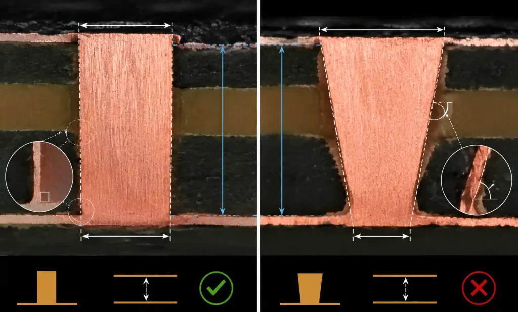
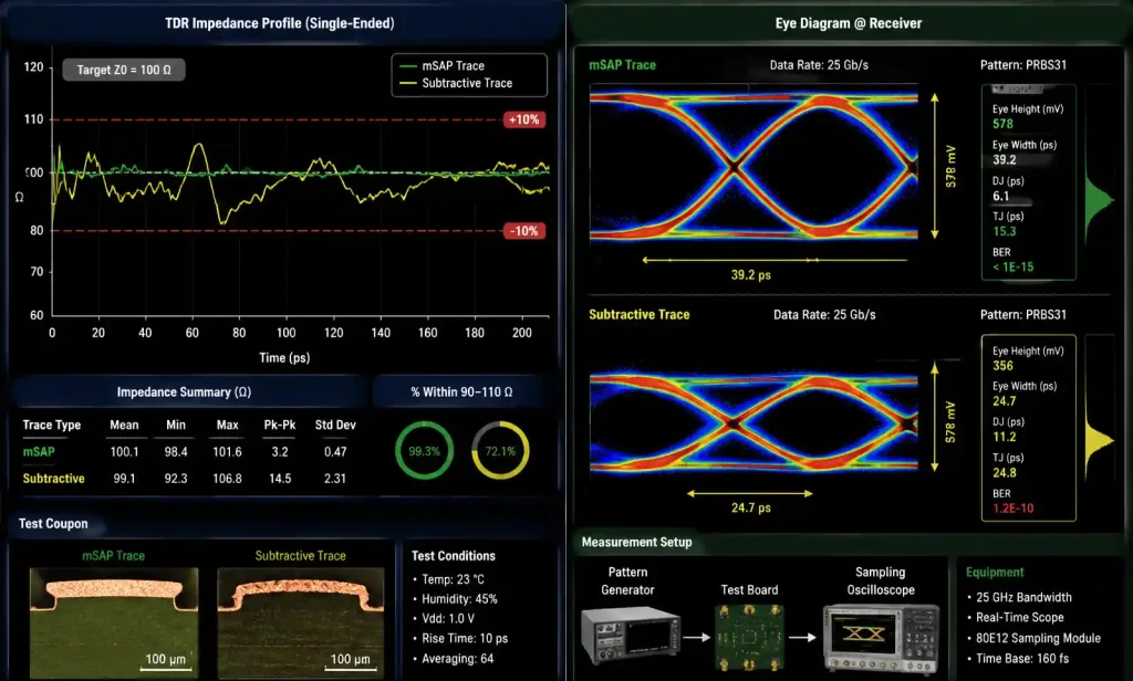
Impedance control: Near-vertical sidewalls and rectangular profiles mean consistent impedance. Hold ±5% tolerance versus ±10-12% with conventional processes. For 100Ω differential pairs on 8-layer stackups, this directly translates to better eye margin at the receiver.
Smaller microvias: Support capture pads down to 150μm with 100μm finished holes. Fine trace capability means you can minimize annular ring while maintaining IPC Class 2/3 requirements. That means more aggressive via placement and better fanout.
Signal integrity: Shorter routing paths, reduced via stubs, and fewer discontinuities. Return path inductance drops, crosstalk decreases, and insertion loss improves—measurable benefits above 10 GHz.
Material utilization: Less copper etched away means less chemical waste. Thinner seed layer also improves plating uniformity for through-hole vias.
Design Rules and Manufacturing Capabilities
| Parameter | Subtractive | Conventional SAP | mSAP | Unit |
|---|---|---|---|---|
| Min trace width | 75 | 50 | 25-30 | μm |
| Min trace spacing | 75 | 50 | 25-30 | μm |
| Microvia diameter | 100-150 | 80-100 | 50-80 | μm |
| Capture pad diameter | 250 | 200 | 150 | μm |
| Min annular ring | 50 | 40 | 25 | μm |
| Trace width tolerance | ±25 | ±10 | ±5 | μm |
| Aspect ratio | 1:1 | 1:1 | 0.8:1 | — |
| Layer count capability | 4-20 | 8-24 | 10-30+ | layers |
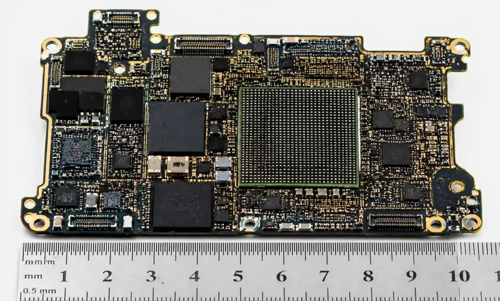
For a typical smartphone main board with 0.4mm pitch BGAs, mSAP lets you route three or four traces between adjacent balls versus only two. This often eliminates one or two signal layers—reducing material cost and improving manufacturability despite higher per-layer fabrication cost.
mSAP vs Subtractive Methods
| Factor | mSAP | Subtractive | Design Impact |
|---|---|---|---|
| Fine line capability | Excellent (25-30μm) | Limited (75-100μm) | Higher density, layer count reduction |
| Trace profile | Rectangular, vertical walls | Trapezoidal, undercut | Better impedance control |
| Process complexity | Higher (7-9 steps) | Lower (5-6 steps) | Longer lead time, higher NRE |
| Cost per layer | 1.5-2.0× | 1.0× | Offset by fewer layers needed |
| Via-in-pad capability | Excellent | Moderate | Direct BGA fanout |
| Material compatibility | Requires smooth Cu foil | Standard RTF/HVLP | Affects adhesion and yield |
| Dimensional stability | Excellent | Good | Critical for fine-pitch BGAs |
Bottom line: A 10-layer mSAP board often costs less and performs better than a 12-layer subtractive board achieving equivalent routing density. For volumes above 10K/year, layer count savings typically justify the higher per-layer cost within the first year.
High-frequency designs above 10 GHz with insertion loss budgets under -15dB benefit significantly from mSAP’s impedance control and reduced via stub effects. Cost-sensitive consumer products with relaxed electrical specs may not justify it unless board size reduction is the primary goal.
DFM Guidelines for mSAP
Trace width/spacing: 25/25μm is possible, but 30/30μm or 35/35μm improves yield and reduces cost. Reserve ultra-fine for critical fanout areas. Maintain consistent trace widths—frequent transitions complicate resist patterning and plating uniformity.
Microvia design: Specify 75-100μm laser via diameters for optimal aspect ratio and plating reliability. For stacked vias, offset by at least half the capture pad diameter to prevent drilling breakthrough. Use via-in-pad with copper fill and planarization for BGA fanout.
Copper balance: Keep copper distribution within 30-40% per layer. Avoid large pours on one side. Use thieving patterns in low-density areas to equalize plating current distribution.
Impedance control: Specify ±5-7% tolerances. Provide clear stackup documentation—dielectric thickness, copper weight, trace geometry. Maintain consistent coupling along differential pairs; discontinuities at vias hit impedance harder at fine geometries.
Panelization: Coordinate panel size and layout with your fabricator—mSAP may have preferred panel dimensions due to plating bath constraints. Allow 3-5mm clearance margins for break-away tabs and V-cut scoring.
Testing: Build in TDR or VNA test points. Request cross-section analysis for qualification builds. For production, flying probe or fixture-based test verifies continuity and isolation.
Common DFM errors to avoid: Specifying tighter geometries than necessary, neglecting copper balancing, inadequate clearance around stacked microvias, missing impedance documentation, and failing to coordinate via fill/planarization with your fabricator’s capability.
FAQ
What is the minimum layer count where mSAP becomes cost-effective?
Typically 8-10 layers for designs requiring sub-50μm line/space. The higher per-layer cost is offset by eliminating 1-2 layers through improved routing density. For prototypes (<100 units), break-even shifts to 10-12 layers due to NRE costs.
Can mSAP be mixed with traditional subtractive layers in the same stackup?
Yes. Hybrid stackups using mSAP for outer layers or high-density cores combined with subtractive inner layers are common. Coordinate with your fabricator on layer sequencing and material compatibility.
How does mSAP affect board thickness and weight?
Often reduces overall thickness by 10-20% by eliminating 1-2 layers for equivalent functionality. Thinner copper foil also contributes marginally to weight savings. For a 10-layer smartphone board, expect 0.1-0.2mm thickness reduction.
What is the typical lead time premium for mSAP fabrication?
Expect 1-2 weeks additional lead time for prototypes due to extra process steps and CAM engineering review. Production lead times approach standard HDI timelines once qualified. Expedited 5-7 day prototypes are available at significant cost premiums.
Does mSAP require different design software?
No specialized EDA tools required. Ensure your software supports DRC down to 25μm and can generate accurate Gerber/ODB++ with layer stackup data. Most modern tools (Altium, Cadence, Mentor, KiCad) handle mSAP rules without modification.
What IPC class requirements apply to mSAP Any Layer HDI?
Typically IPC-6012 Class 2 or Class 3. Fine geometries don’t change class requirements, but meeting Class 3 annular ring, test, and microsectioning criteria requires tighter process control. Discuss with your fabricator during DFM review.
How does material selection differ for mSAP?
Requires smooth copper foil (VLP or ultra-low-profile) to achieve target line widths. Dielectric material must provide adequate adhesion to smooth copper—modified resin systems or surface treatments are common. Typical materials: Panasonic Megtron 6, Isola IS620, or Shengyi S1000-2M.
Can mSAP support controlled depth milling for component embedding?
Yes. mSAP is compatible with cavity milling for embedding passives or thin ICs. The sequential build-up nature of Any Layer HDI aligns well with component embedding. Coordinate via placement around cavities to maintain structural integrity.
Conclusion
mSAP-based Any Layer HDI delivers measurable advantages for applications demanding maximum routing density, superior signal integrity, or aggressive miniaturization. Ultra-fine line capability, near-vertical trace profiles, and tight dimensional tolerances enable designs that are impossible or impractical with subtractive processes.
When evaluating mSAP, focus on total system cost—layer count, board size, and electrical performance—rather than per-layer fabrication cost alone. Collaborate early with your PCB fabricator to align design rules with their specific mSAP capabilities. Submit complete stackup documentation, impedance requirements, and via specifications to streamline CAM engineering review and ensure first-pass success.
For designers working with HDI flex or rigid-flex structures where mSAP is combined with flexible substrates, our HDI flex PCB 3+N+3 structure guide covers additional considerations for bendable designs. Before releasing your design, run the DFM checklist and request cross-section analysis for qualification builds to validate microvia formation, trace geometry, and layer registration. For complex designs, get a complimentary design review from your fabricator’s CAM team.