
HDI PCB Manufacturing Services: Complete Guide for Electronic Device Manufacturers
If you want to design compact, high-performance electronic devices, you need to understand HDI PCB manufacturing capabilities, via structures, and quality standards that enable miniaturization without compromising reliability. HDI technology has become the backbone of modern electronics – smartphones, wearables, medical devices, and automotive systems all rely on it. This guide covers what you need to evaluate HDI PCB manufacturers, understand cost drivers, and specify the right configuration for your project.
What Is HDI PCB Manufacturing?
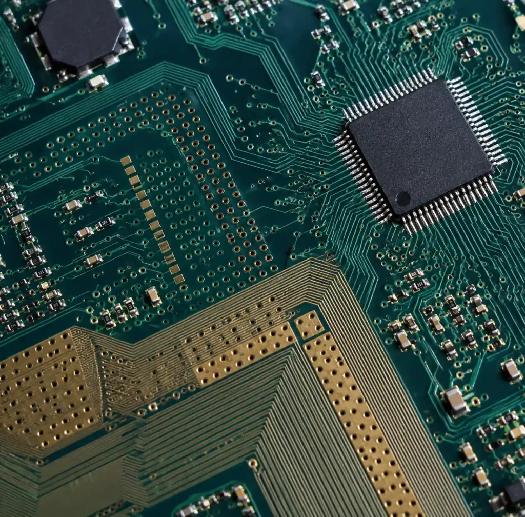
HDI PCB is a high-density interconnect board with microvias (laser-drilled holes under 0.15mm), fine-pitch traces, and advanced layer stackups that enable superior component density compared to conventional PCBs. Microvia technology allows routing between any layer pairs while maintaining signal integrity for high-speed digital and RF applications.
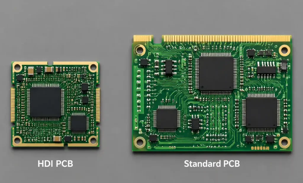
HDI uses sequential lamination to build up layers with buried and blind vias. You can achieve trace widths as fine as 3mil (75μm) and via sizes down to 0.1mm – versus 5mil traces and 0.3mm mechanical drills in standard boards. This reduces board size by up to 40% while improving electrical performance through shorter signal paths and lower EMI.
HDI Via Types and Structures
Understanding via types is critical because they determine routing flexibility, layer count, and cost.
Blind vias connect an outer layer to inner layers without penetrating the entire board. They allow surface mount components to sit over via locations, adding 15-25% to cost but providing significant routing density benefits.
Buried vias connect inner layers only and remain hidden within the stackup. They don’t consume surface area, maximizing space for components and routing. Manufacturing requires sequential lamination – inner layer pairs are drilled, plated, and laminated before adding outer layers.
Microvias are laser-drilled blind vias with diameters between 0.075mm and 0.15mm. They can be stacked (aligned vertically) or staggered (offset between layers). Stacked vias provide direct vertical connections but require tighter registration; staggered vias distribute stress better for thermal cycling applications.
HDI PCB Manufacturing Process
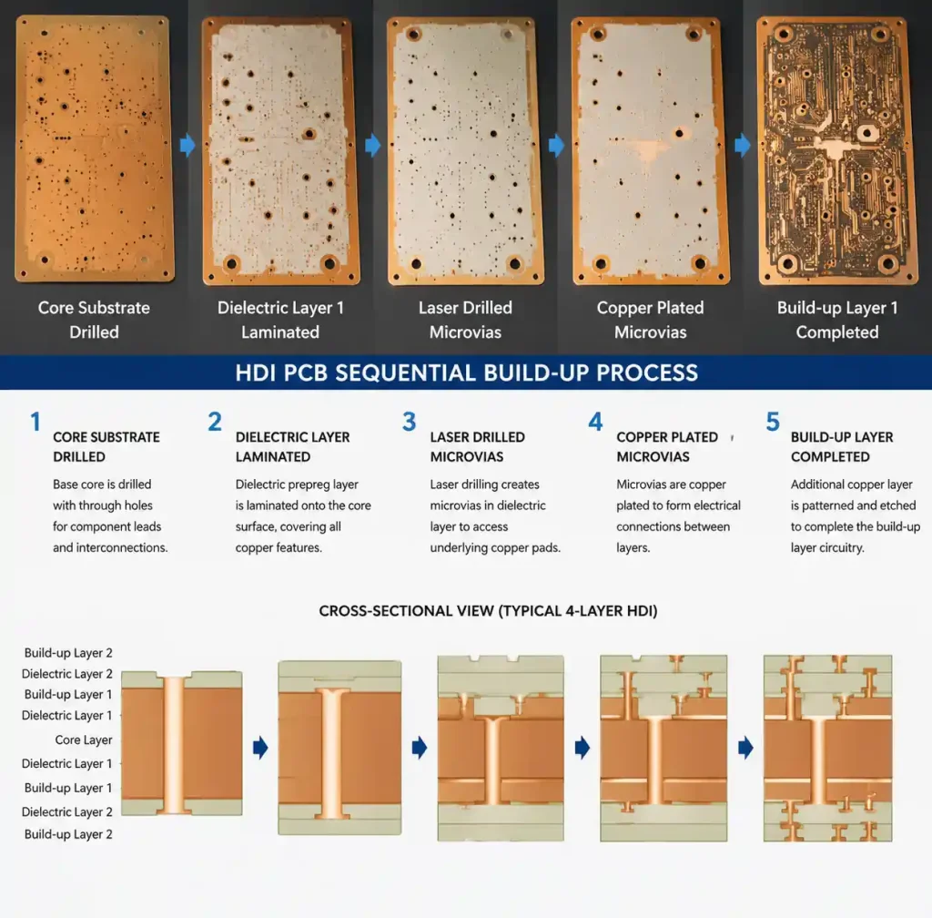
HDI manufacturing differs fundamentally from standard PCB fabrication due to sequential build-up and laser drilling.
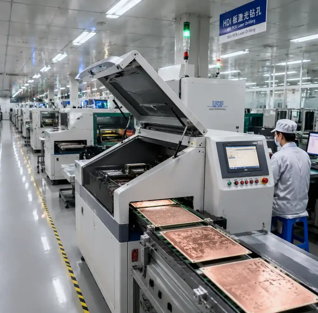
The process starts with a core substrate (typically 2-4 layer FR-4) with through-hole vias connecting core layers. After patterning inner layer copper, manufacturers apply a thin dielectric layer (50-100μm) using resin-coated copper or photodielectric films. Laser drilling creates microvias through this dielectric – CO2 or UV lasers ablate material in precise locations guided by CAM data.
After laser drilling, copper plating fills the microvias and forms the circuit pattern on the build-up layer. This sequence repeats for each additional build-up layer until reaching the specified layer count. Finally, solder mask, surface finish, and electrical testing complete the process.
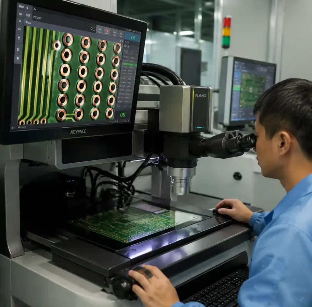
You should verify that your HDI manufacturer has automated laser drilling with vision alignment – registration accuracy directly affects microvia reliability and yield. Manufacturing tolerances of ±25μm are standard for production HDI boards meeting IPC-6012 Class 3.
HDI PCB vs Standard PCB
Understanding performance and cost differences helps you make informed design decisions.
| Parameter | HDI PCB | Standard PCB |
|---|---|---|
| Via Type | Microvias, blind, buried (laser-drilled) | Through-hole only (mechanical drill) |
| Min Via Size | 0.075-0.15mm | 0.3mm |
| Min Trace/Space | 3/3 mil (75/75μm) | 5/5 mil (125/125μm) |
| Typical Layer Count | 4-20+ layers | 2-12 layers |
| Component Density | Very high (fine-pitch BGAs, 0201) | Standard (QFP, 0402) |
| Signal Integrity | Excellent (shorter paths) | Good (longer paths) |
| Board Size Reduction | 30-40% smaller | Standard size |
| Cost | Higher (complex process) | Lower (standard process) |
| Lead Time | 10-15 days typical | 5-10 days typical |
Choose HDI when your design requires component pitch below 0.5mm, board thickness under 1.0mm, or signal frequencies above 1 GHz. Standard PCBs remain cost-effective for larger form factors and lower density.
Cost Factors in HDI PCB Manufacturing
Layer count directly impacts cost – a 1+6+1 structure costs 40-60% more than an 8-layer standard board. More complex 2+6+2 or any-layer configurations increase costs further. You can reduce costs by minimizing build-up layers while meeting routing density.
Via type and count matter. Microvias and blind vias cost more than through-hole vias. Stacked microvias add 15-20% over staggered designs due to tighter registration requirements.
Board size and panelization affect per-unit costs. Smaller boards allow more efficient panelization – a 50×50mm board might fit 48 pieces per panel versus 12 for 100×100mm. Optimize board dimensions to maximize panel utilization (standard panels are 18″×24″).
Materials and surface finish add costs – low-loss dielectrics or high-Tg substrates add 20-35%, and ENIG finish adds $5-15 per board. Volume shows significant economies of scale: prototypes (5-10 boards) might cost $100-200 each, while production volumes (1000+ units) drop to $20-40 per board.
| Specification | Cost Impact | Optimization Strategy |
|---|---|---|
| Layer Count | +40% per build-up layer pair | Minimize build-up layers |
| Via Type | Stacked vias +15-20% | Use staggered when possible |
| Board Size | Larger = higher unit cost | Optimize for panel utilization |
| Materials | High-Tg/low-loss +20-35% | Specify only where required |
| Surface Finish | ENIG +$5-15 per board | Match to application needs |
| Volume | 5× difference proto to production | Plan production volumes early |
Quality Standards and IPC-6012 Class 3
IPC-6012 is the primary qualification standard for rigid PCBs, including HDI boards. It defines three quality classes:
Class 2 applies to dedicated service equipment where high performance is required but downtime is not critical – most consumer electronics HDI boards.
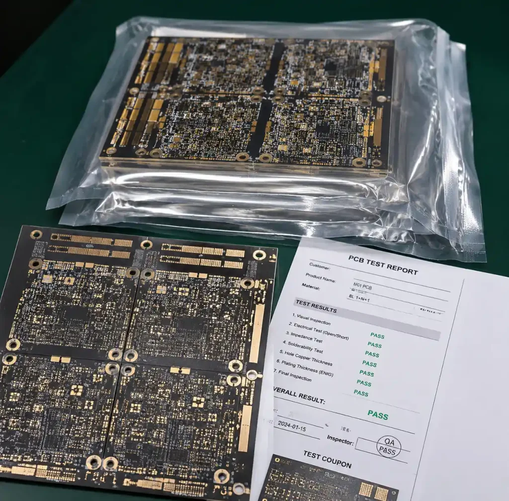
Class 3 applies to products where continued performance is critical and downtime cannot be tolerated – medical devices, aerospace, military. For HDI boards, Class 3 requirements include: minimum microvia fill of 75% depth, no voids exceeding 20% of via cross-section, copper uniformity within ±20%, via registration within ±50μm, and cleanliness below 1.56 μg/cm² ionic contamination.
Specify Class 3 for medical, automotive safety, or any application where field failures create liability. It adds 15-25% to cost but significantly improves reliability.
Additional relevant standards: IPC-2221 (PCB design), IPC-2226 (HDI design), IPC-A-610 (assembly acceptability), ISO 9001, IATF 16949 (automotive), ISO 13485 (medical). Verify your manufacturer holds current certifications for your industry.
Applications of HDI PCBs
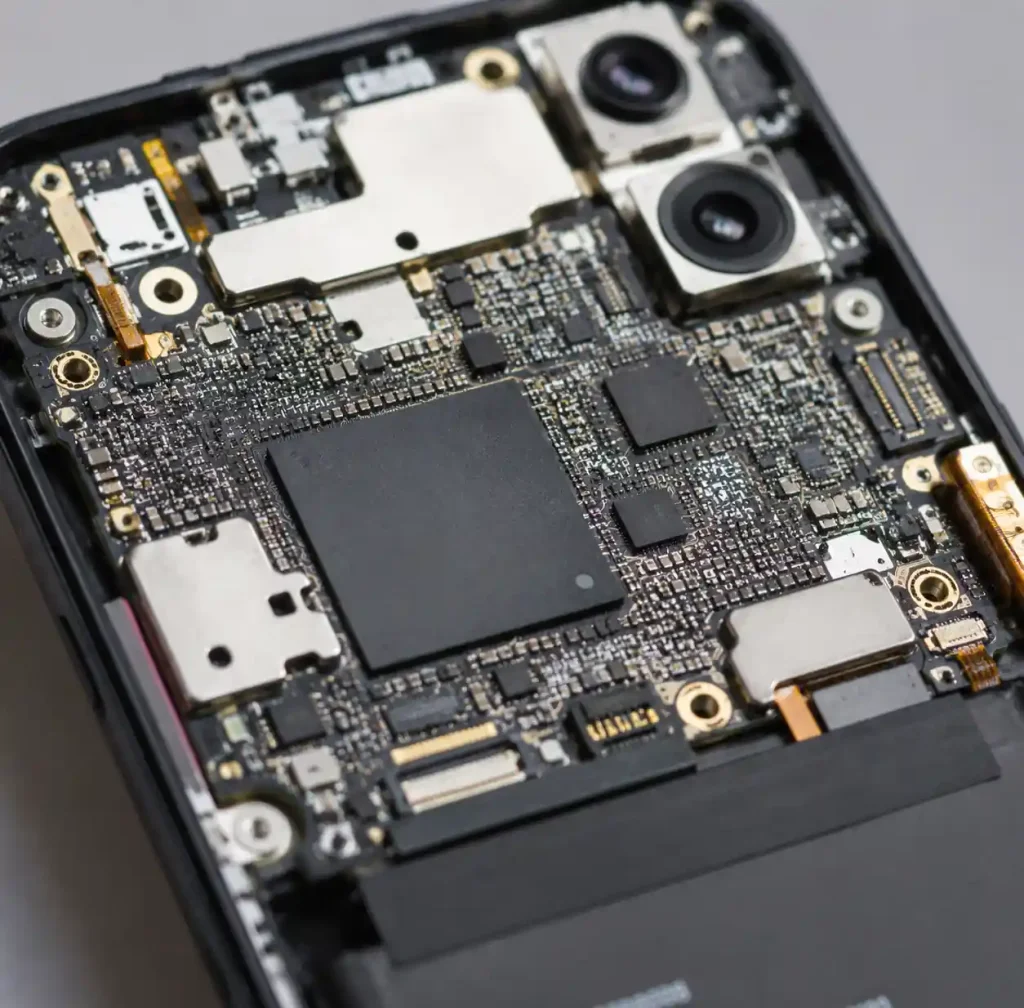
Smartphones and tablets use 8-12 layer HDI configurations with microvias for component density. Fine-pitch BGAs with 0.4mm pitch mount over staggered microvias.
Wearable devices use rigid-flex HDI constructions combining flexible interconnects with HDI rigid sections. Explore Rigid-Flex PCB solutions for these applications.
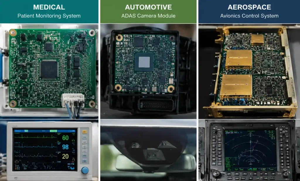
Medical devices demand IPC-6012 Class 3 quality with 10+ year service life. HDI enables miniature implantable devices while meeting biocompatibility requirements.
Automotive electronics (ADAS, infotainment, EV battery management) require survival from -40°C to +125°C with IATF 16949 quality standards.
Aerospace and defense use high-layer-count HDI (16-24 layers) with controlled impedance for phased array radar and satellite communication systems.
How to Select an HDI PCB Manufacturer
Technical capabilities: Verify layer count capability (4-12 layers typical, 12-24 advanced), via technology support (blind, buried, stacked, staggered), minimum trace/space (3/3 mil), and board size range.
Manufacturing process: Check laser drilling systems (automated UV or CO2 with vision alignment), sequential lamination presses, impedance control testing (±10% or ±5Ω), and inspection capabilities (flying probe, X-ray, microsectioning).
Quality certifications: IPC-6012 (Class 2 or 3), ISO 9001, IATF 16949 (automotive), ISO 13485 (medical), UL certification.
Production capacity: Verify monthly capacity, lead times (prototypes 7-10 days, production 10-15 days), and expedited service availability.
Engineering support: Look for DFM review, stackup design assistance, impedance calculation, and comprehensive fabrication drawings.
At Andwin Circuits, we offer comprehensive PCB assembly services with HDI manufacturing up to 50 layers and 7-day prototypes, with ISO 9001, IATF 16949, and UL certifications.
Lead Time Considerations
HDI lead times typically range from 7 days for quick-turn prototypes to 15-20 days for complex production builds. Factors affecting turnaround:
- Design complexity: Simple 1+6+1 with staggered microvias ships faster than any-layer with stacked vias – each build-up layer adds 2-3 days.
- Material availability: Standard FR-4 ships immediately; specialized high-Tg or low-loss may take 3-5 days.
- Testing requirements: Basic electrical adds 1 day; comprehensive impedance, microsectioning, and reliability add 3-5 days.
- Manufacturing queue: Orders received early in the week ship faster than those just after batch cutoff.
You can reduce lead times by submitting complete DFM-verified designs, specifying standard materials when possible, planning around production schedules, and using quick turn PCB assembly for urgent projects.
FAQ
What is the minimum layer count for HDI PCBs?
HDI typically starts at 4 layers (1+2+1 structure) with one microvia build-up layer on each side of a 2-layer core. Most practical applications use 6-12 layers to fully leverage the routing density benefits.
How much does HDI PCB manufacturing cost compared to standard PCBs?
HDI costs 40-80% more than equivalent-layer-count standard boards due to sequential lamination and laser drilling. Prototypes (5-10 boards) run $100-200 each; production volumes (1000+ units) drop to $20-40 per board depending on specs.
What’s the difference between blind vias and buried vias?
Blind vias connect an outer layer to inner layers without penetrating the entire board, remaining visible from one surface. Buried vias connect only inner layers and stay hidden within the stackup. Blind vias let surface components mount over via locations; buried vias maximize surface routing area.
Can HDI PCBs be used for high-temperature applications?
Yes, with appropriate materials. Standard FR-4 works up to 130°C; high-Tg substrates extend to 170°C or higher. Specify high-Tg (Tg ≥ 170°C) for automotive, industrial, or aerospace applications with extended temperature exposure.
What IPC standard applies to HDI PCB manufacturing?
IPC-6012 covers rigid PCB qualification including HDI boards. IPC-2226 provides HDI/microvia design guidance. IPC-A-610 defines assembly acceptance. Most commercial HDI boards meet IPC-6012 Class 2; medical, automotive, and aerospace require Class 3.
Conclusion
HDI PCB manufacturing enables the compact, high-performance devices that define modern technology. Understanding via types, manufacturing processes, quality standards, and cost factors helps you make informed decisions. The key to success lies in early manufacturer engagement for DFM review, realistic lead time planning, and clear quality specifications. Whether you need IPC-6012 Class 2 or Class 3, selecting a manufacturer with proven HDI capabilities and industry certifications ensures reliable production. If you need high-quality HDI PCBs, Andwin Circuits offers advanced manufacturing up to 50 layers with 7-day prototypes, certified to ISO 9001, IATF 16949, and UL standards. Contact us today for custom HDI solutions and competitive pricing.