
AMB Ceramic PCB Technology: Active Metal Brazing for Si3N4 Substrates Explained
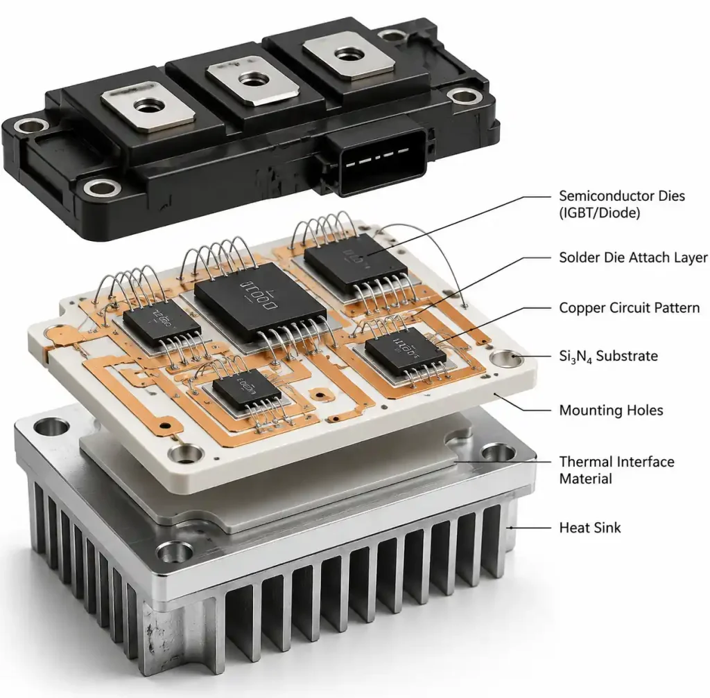
Active Metal Brazing (AMB) is a game-changer for ceramic PCBs in high-power electronics – IGBT modules, EV inverters, RF amps, you name it. The bond between copper and silicon nitride (Si3N4) hits over 300 MPa shear strength, which means it survives thermal cycling that would kill standard DBC boards. This guide covers the AMB process, why Si3N4 beats Al2O3 for power applications, design rules we’ve learned from production, and when to spec AMB over alternatives.
Active Metal Brazing Technology: How It Works
AMB and DBC (Direct Bonded Copper) bond differently. DBC relies on eutectic bonding at 1065-1083°C for Al2O3. AMB uses a brazing alloy with active metals – titanium, zirconium, or hafnium – that chemically react with the ceramic surface.
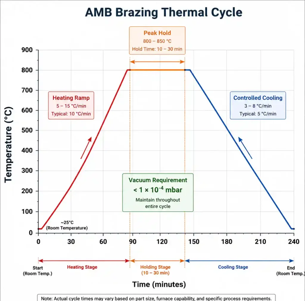
The process: copper foil (0.3-1.0 mm thick) goes on both sides of the Si3N4 substrate. The brazing alloy – typically AgCuTi (68.8% Ag, 26.7% Cu, 4.5% Ti) – sits between the copper and ceramic. The whole stack heats in a vacuum furnace to 800-850°C, well below Si3N4’s melting point but hot enough to activate the titanium.
During brazing, titanium diffuses to the ceramic interface and forms titanium nitride (TiN) and titanium silicide compounds. These reaction layers chemically bond to the Si3N4, while the silver-copper matrix provides ductility to handle thermal expansion mismatch. This dual mechanism – chemical bond plus ductile layer – is why AMB joints survive extreme thermal cycling without delamination.
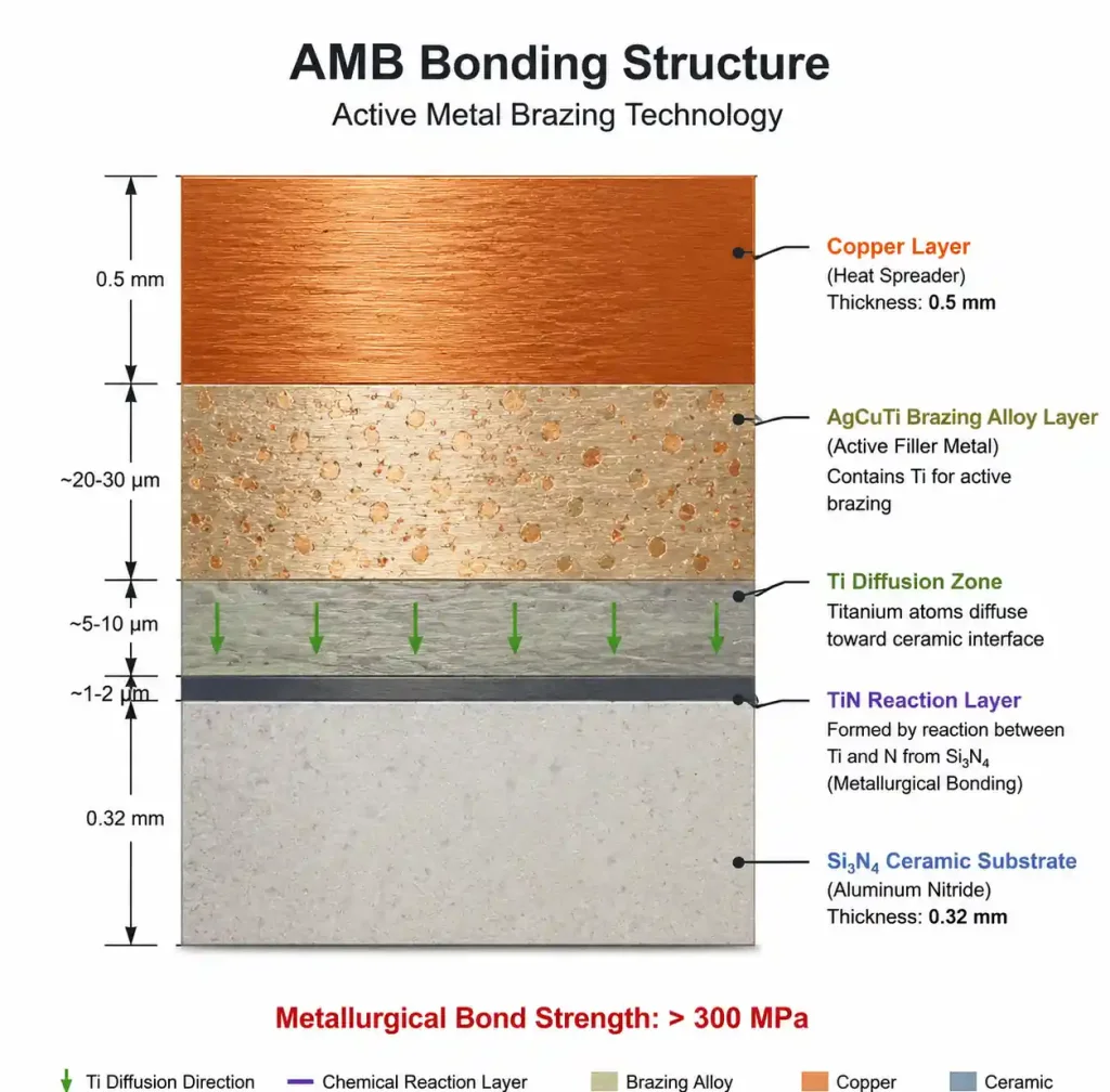
The result: copper layers bonded at >300 MPa shear strength, compared to 200-250 MPa for DBC on Al2O3. And AMB holds through -55°C to +250°C temperature excursions, making it suitable for automotive and aerospace power electronics.
Why Silicon Nitride (Si3N4) for High-Power Applications
Si3N4 is the go-to ceramic for demanding power electronics because of its thermal, mechanical, and electrical properties.
Thermal conductivity is the main driver. Si3N4 runs 80-90 W/mK versus 24-28 W/mK for Al2O3 (96% alumina). That 3× improvement in heat spreading lowers junction temperatures. For a 500W IGBT module, switching from Al2O3 to Si3N4 can drop junction temp by 20-30°C – better reliability and higher power density.
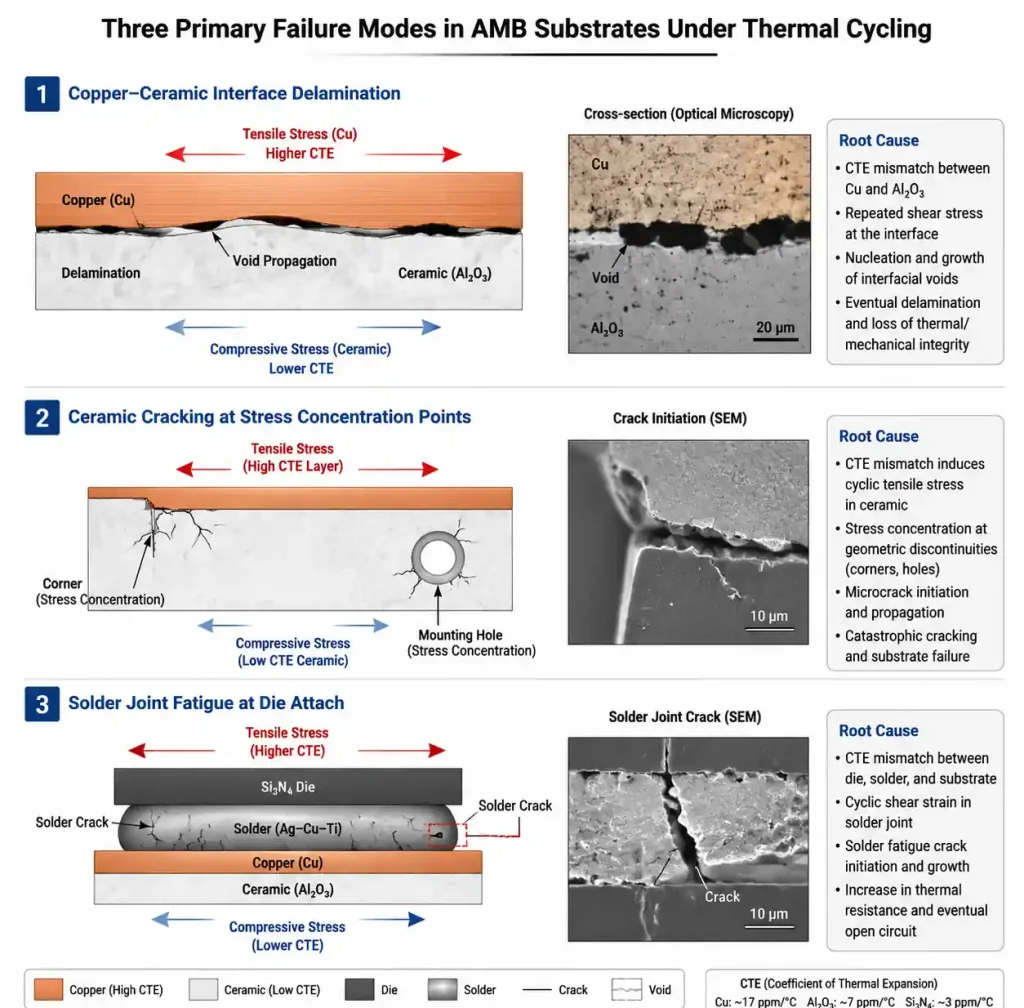
Fracture toughness is just as critical. Si3N4 hits 5-7 MPa·m^½, roughly double Al2O3’s 3-4 MPa·m^½. This reduces catastrophic failure from thermal shock, assembly stress, or vibration. In power modules with 1000+ thermal cycles (-40°C to +150°C), Si3N4 substrates show much lower crack propagation.
CTE matching matters too. Si3N4’s CTE is 3.2-3.4 ppm/°C, closer to silicon (2.6 ppm/°C) and copper (17 ppm/°C) than Al2O3’s 6.8 ppm/°C. Less CTE mismatch means lower thermal stress at the copper-ceramic interface during temperature cycling.
Dielectric strength stays excellent – >15 kV/mm at 0.32 mm thickness, enough for 3.3 kV and 6.5 kV power modules in EV inverters and industrial drives.
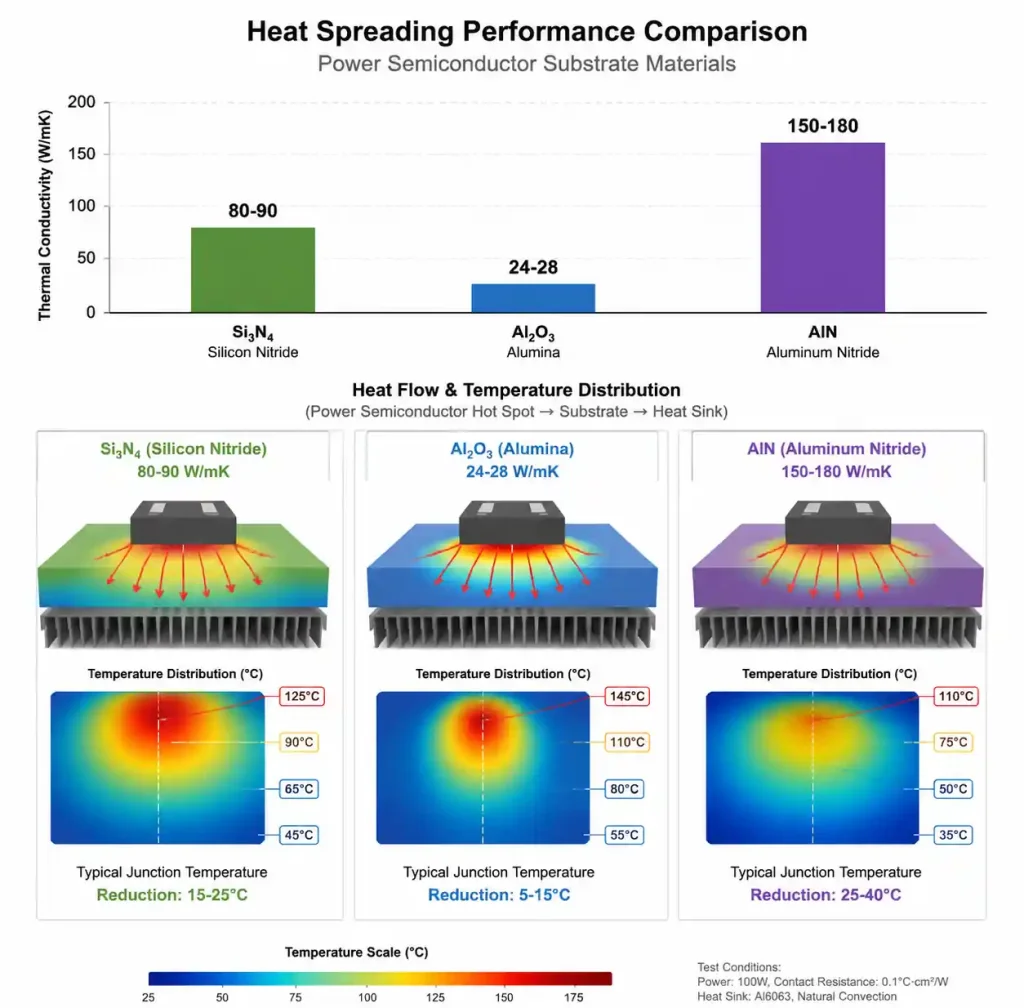
Technical Parameter Comparison: Si3N4 vs. Al2O3 vs. AlN
Here’s how these materials stack up for power electronics:
| Parameter | Si3N4 (AMB) | Al2O3 (DBC) | AlN (AMB/DBC) |
|---|---|---|---|
| Thermal Conductivity | 80-90 W/mK | 24-28 W/mK | 150-180 W/mK |
| Fracture Toughness | 5-7 MPa·m^½ | 3-4 MPa·m^½ | 3-4 MPa·m^½ |
| Flexural Strength | 600-800 MPa | 300-400 MPa | 300-350 MPa |
| CTE (25-400°C) | 3.2-3.4 ppm/°C | 6.8 ppm/°C | 4.5 ppm/°C |
| Dielectric Strength | >15 kV/mm | >12 kV/mm | >14 kV/mm |
| Dielectric Constant (εr) | 7.0-8.0 | 9.5-10.0 | 8.5-9.0 |
| Relative Cost | 1.8-2.2× | 1.0× | 3.5-4.5× |
| Typical Substrate Thickness | 0.32, 0.50, 0.635 mm | 0.38, 0.635 mm | 0.635, 1.0 mm |
Si3N4 hits the sweet spot for high-reliability power electronics. AlN gives better thermal conductivity but at 3.5-4.5× the cost and lower fracture toughness. Si3N4 delivers 70% of AlN’s thermal performance at 45% of the cost, with significantly better mechanical reliability.
For automotive power modules, that toughness and flexural strength (600-800 MPa vs 300-400 MPa) are decisive. EV inverters see continuous thermal cycling, vibration, and shock loads. Si3N4 gives you safety margin that Al2O3 can’t match.
The CTE advantage also boosts solder joint reliability. Closer CTE match to copper means less thermal stress in solder joints during temperature cycling – lifetimes exceeding 100,000 cycles in -40°C to +150°C accelerated testing.
AMB Process Parameters and Bond Quality
The AMB manufacturing process affects bond strength, adhesion, and long-term reliability. Here are the key parameters:
| Process Parameter | Typical Range | Impact on Quality | Critical Control Point |
|---|---|---|---|
| Brazing Temperature | 800-850°C | Too low: incomplete Ti reaction; too high: excessive Ti diffusion | ±5°C control required |
| Vacuum Level | 1×10^-4 to 5×10^-5 mbar | Prevents oxidation of active metals | Must reach <1×10^-4 before heating |
| Heating Rate | 5-15°C/min | Too fast: thermal stress cracking | Ramp control in furnace program |
| Hold Time at Peak Temperature | 10-30 minutes | Ensures complete Ti-ceramic reaction | Based on substrate thickness |
| Cooling Rate | 3-8°C/min | Controls residual stress formation | Critical for thick copper (>0.6mm) |
| Copper Layer Thickness | 0.3-1.0 mm | Thicker copper = higher thermal stress | Design trade-off: conductivity vs. stress |
| AgCuTi Foil Thickness | 25-75 μm | Affects bond line thickness and ductility | 50 μm typical for 0.32mm substrate |
The titanium content in the brazing alloy is the critical variable. 4.5% Ti in AgCuTi gives enough titanium to form the TiN reaction layer, with excess staying in the matrix for ongoing chemical stability. Below 3.5% Ti, bonding strength drops significantly. Above 6%, the alloy becomes brittle.
Copper thickness trade-off: Thicker copper (0.8-1.0 mm) improves current capacity but increases thermal stress from CTE mismatch. For Si3N4, 0.5-0.635 mm copper is the sweet spot for most power applications. Go thicker (>0.8 mm) only for >200A continuous current or multiple etching steps.
Surface finish on the ceramic before brazing is non-negotiable – Ra <0.4 μm for uniform contact with the brazing foil. Any contamination creates voids that nucleate delamination failures. Standard cleaning: ultrasonic in deionized water followed by vacuum baking at 150°C.
Design Guidelines for AMB Si3N4 Substrates
Designing with AMB ceramic substrates means different rules than FR4 or metal-core PCBs. For applications requiring both high current and effective thermal management, many engineers combine heavy copper and metal core PCB solutions – similar thermal principles apply.
Minimum trace width and clearance: For signal traces, 0.3 mm minimum. For power traces >10A, 0.5 mm minimum. These account for etching tolerances on thick copper (0.3-0.635 mm). For 3.3 kV modules on 0.32 mm Si3N4, trace-to-trace clearance should be 3.0 mm minimum. For 6.5 kV, bump to 6.5 mm – this includes margin for altitude derating and contamination.
Thermal management: Unlike FR4, avoid large solid copper areas (>100 cm²) unless absolutely necessary. If you need them, add stress relief slots to allow differential expansion. Keep copper patterns as symmetrical as possible – top and bottom copper area should match within 15% to prevent bending stress.
Vias and mounting holes: Minimum hole diameter is 0.5 mm for mechanical drilling, 0.2 mm for laser. Hole-to-edge distance should be at least 2× substrate thickness. Mounting holes for power modules: use minimum 3.0 mm diameter (4.0 mm preferred) with 0.5 mm copper clearance around the hole.
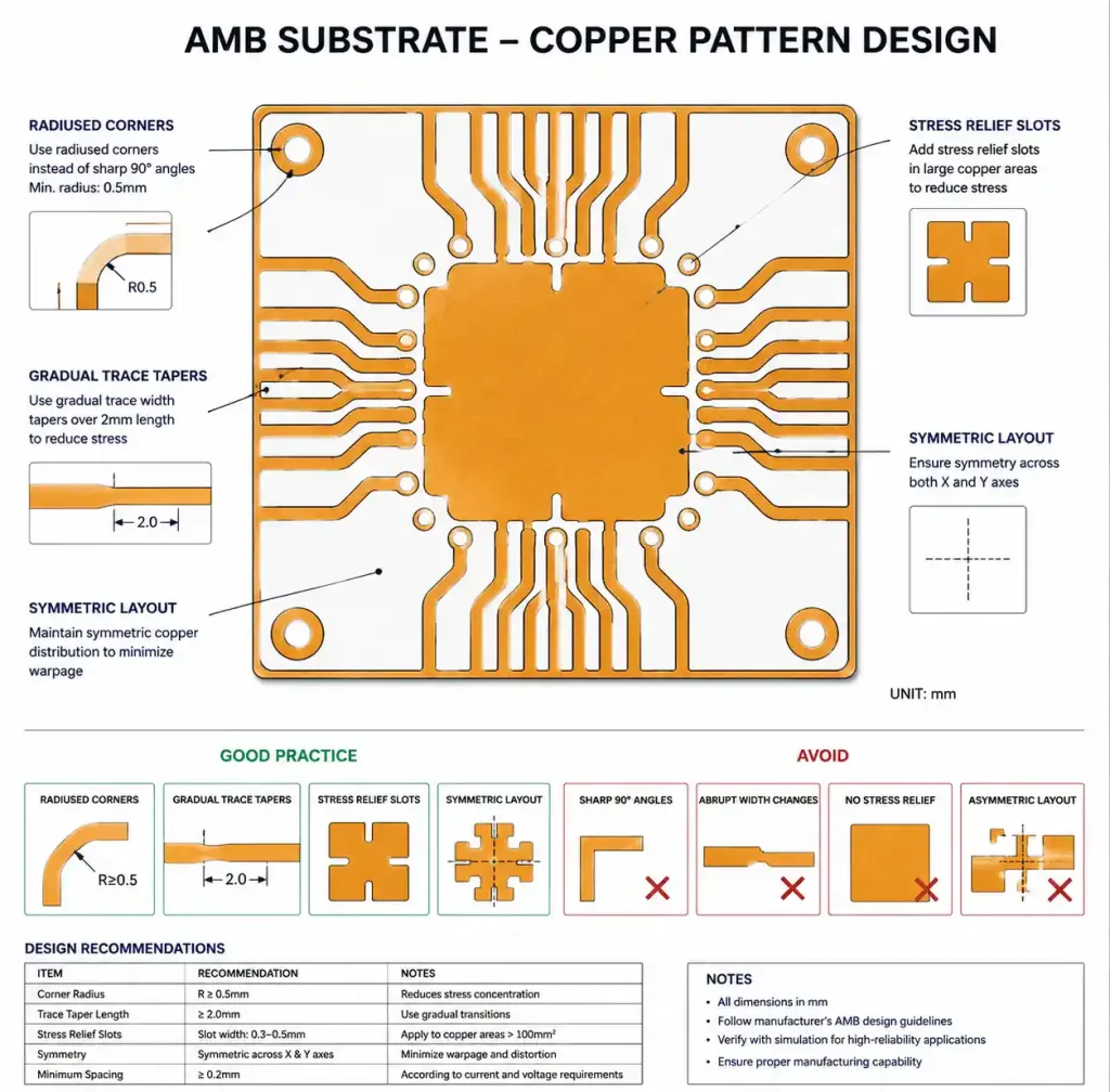
DFM for reliability: Avoid sharp corners – use 45° chamfers or 0.5 mm radius at trace junctions. Where traces transition from wide to narrow, use gradual tapers over at least 2 mm. These details prevent stress concentration during thermal cycling.
AMB vs. DBC vs. Thick-Film: Technology Comparison
When do you pick AMB over DBC or thick-film? Here’s the decision matrix:
| Factor | AMB on Si3N4 | DBC on Al2O3 | DBC on AlN | Thick-Film on Al2O3 |
|---|---|---|---|---|
| Thermal Conductivity | 80-90 W/mK | 24-28 W/mK | 150-180 W/mK | 24-28 W/mK |
| Bond Strength | 300+ MPa | 200-250 MPa | 250+ MPa | 40-80 MPa |
| Thermal Cycling Reliability | Excellent (100k+ cycles) | Good (50k-80k cycles) | Excellent (100k+ cycles) | Limited (10k-20k cycles) |
| Minimum Trace Width | 0.3 mm | 0.5 mm | 0.5 mm | 0.15 mm |
| Copper Layer Thickness | 0.3-1.0 mm | 0.3-0.635 mm | 0.3-0.635 mm | 0.010-0.025 mm |
| Voltage Rating | Up to 6.5 kV | Up to 3.3 kV | Up to 6.5 kV | Up to 1.5 kV |
| Relative Cost | 1.8-2.2× | 1.0× | 3.5-4.5× | 0.6-0.8× |
| Typical Lead Time | 3-5 weeks | 2-3 weeks | 4-6 weeks | 1-2 weeks |
AMB on Si3N4 is the right choice when: thermal management is critical but AlN cost is prohibitive, thermal cycling exceeds 50,000 cycles (automotive, renewable energy), you need thick copper (>0.5 mm) for high current, or mechanical reliability in harsh environments is required.
DBC on Al2O3 is still the standard for cost-sensitive applications with moderate thermal requirements (<100W per substrate).
Thick-film only makes sense for low-power (<50W), quick-turn prototypes, or specialized fine-line work.
FAQ
What is the typical lead time for AMB Si3N4 substrate manufacturing?
Prototypes (10-50 pieces) run 3-5 weeks. Production volumes (500+ pieces) take 4-6 weeks. The AMB process itself is 2-3 days, but ceramic prep, vacuum brazing, inspection, and etching add time. Expedited 2-week service is available from some shops at 50-80% premium.
Can AMB substrates run above 200°C continuously?
Yes, AMB on Si3N4 is rated for continuous operation up to 250°C ambient. The AgCuTi braze alloy stays stable well beyond that, and Si3N4 properties don’t degrade. The limiting factor is usually copper oxidation above 250°C in air – protective coatings (OSP, ENIG) can help. For >250°C continuous, check with your manufacturer about specialized treatments.
How do I calculate thermal resistance of an AMB Si3N4 substrate?
Rth = t / (k × A), where t is substrate thickness (m), k is thermal conductivity (W/mK), and A is effective heat spreading area (m²). For 0.32 mm Si3N4 (k=85 W/mK) with 1 cm² die area, Rth ≈ 0.038 K/W. For real designs, run thermal FEA – copper pattern and heatsink interface matter.
Is AMB compatible with standard PCB reflow soldering?
Yes – AMB handles peak reflow temperatures of 260°C (Pb-free SAC305 profile) without degradation. But ceramic has higher thermal mass than FR4, so extend the preheat zone to 90-120 seconds for uniform heating. Wave soldering and manual soldering work fine too.
What inspection methods verify AMB bond integrity?
Good manufacturers run: 100% ultrasonic C-scan for voids/delamination (<5% void area acceptance), 10× visual inspection for surface defects, shear strength testing on coupons (>300 MPa acceptance), and thermal cycling qualification (-40°C to +150°C, 200+ cycles) for new designs. Ask for inspection reports as part of qualification.
Conclusion and Design Recommendations
AMB on Si3N4 delivers the thermal, mechanical, and electrical performance needed for next-gen power electronics – EV inverters, industrial drives, RF power amps. Three things to get right: spec copper thickness based on current needs and thermal stress (0.5-0.635 mm is the sweet spot for most), follow DFM rules to avoid stress concentration (radiused corners, gradual tapers, edge clearance), and validate with thermal cycling before production.
Run the numbers against your requirements. Most engineers find the 80-90 W/mK thermal conductivity and 100,000+ cycle reliability justify the 1.8-2.2× cost premium over Al2O3 DBC – and it’s still cheaper than AlN. For applications with extreme power density, comparing high thermal conductivity aluminum PCB vs metal core PCB helps clarify which thermal solution fits your design. And when designing for EV charging infrastructure with similar thermal demands, our guide on metal core PCB for EV charging systems offers complementary insights on thermal management and layout strategies. For help with your AMB PCB design, upload specs for a free manufacturability review or contact our CAM team about copper thickness optimization and thermal simulation support.