Telecommunication PCB Assembly: 5G Infrastructure Requirements
The deployment of 5G infrastructure demands PCB assemblies that can handle significantly higher frequencies, data rates, and thermal loads compared to previous generations. For telecom equipment manufacturers and PCB design engineers working on base stations, small cells, and massive MIMO systems, understanding the specific design rules and manufacturing requirements is critical to avoiding costly respins and ensuring reliable performance in field deployment.
This guide covers the essential PCB design parameters, material selection criteria, and assembly considerations for 5G telecommunication equipment, with specific focus on frequency ranges up to 40 GHz (FR2) and the manufacturing capabilities required to support these advanced designs.
Table of Contents
- 5G Infrastructure PCB Requirements Overview
- Critical Design Parameters for mmWave and Sub-6 GHz
- Material Selection for High-Frequency Performance
- Multilayer Stackup Design for 5G Applications
- DFM Considerations for Telecommunication PCB Assembly
- Thermal Management and Power Delivery
- FAQ
- Conclusion and Next Steps
1. 5G Infrastructure PCB Requirements Overview
5G network infrastructure operates across two distinct frequency ranges: FR1 (sub-6 GHz) and FR2 (24-40 GHz mmWave). Each range imposes different requirements on PCB design and assembly. Base station radio units, remote radio heads (RRH), and massive MIMO antenna arrays require PCBs that maintain signal integrity at frequencies where traditional FR4 materials show unacceptable loss.
The key challenges for telecommunication PCB assembly in 5G applications include:
Signal integrity at high frequencies: At mmWave frequencies, even minor impedance discontinuities cause significant signal degradation. Trace routing, via design, and connector transitions must be optimized to minimize insertion loss and return loss. For FR2 applications, insertion loss must typically remain below 1 dB per inch at 28 GHz.
Thermal dissipation: 5G base stations generate substantially more heat than 4G equipment due to higher power amplifier requirements and increased processing loads. Active cooling is often necessary, but PCB design must facilitate heat transfer from high-power components. Thermal vias, thick copper layers, and metal-core substrates are frequently required.
Manufacturing precision: High-frequency designs demand tighter tolerances on trace width, spacing, and layer-to-layer registration. What would be acceptable variation in consumer electronics can shift impedance enough to fail specification in 5G radio designs.
The table below summarizes the key differences between PCB requirements for 4G versus 5G infrastructure:
| Parameter | 4G LTE Infrastructure | 5G FR1 (Sub-6 GHz) | 5G FR2 (mmWave) |
|---|---|---|---|
| Operating frequency | Up to 2.6 GHz | Up to 6 GHz | 24-40 GHz |
| Substrate material | Standard FR4 (Dk 4.4) | Low-loss FR4 or mid-loss | PTFE-based (Rogers, Taconic) |
| Loss tangent requirement | <0.02 | <0.01 | <0.004 |
| Impedance tolerance | ±10% | ±7% | ±5% |
| Minimum trace/space | 4/4 mil | 3/3 mil | 2/2 mil |
| Via aspect ratio | 10:1 | 12:1 | 8:1 (HDI preferred) |
| Layer count (typical) | 8-12 layers | 10-16 layers | 12-20 layers |
| Copper weight (signal) | 0.5-1 oz | 0.5 oz | 0.5 oz (0.25 oz for mmWave) |
This comparison illustrates why 5G designs cannot simply reuse 4G design rules. The material properties, tolerances, and manufacturing capabilities required for reliable 5G performance represent a significant step change from previous generations.
2. Critical Design Parameters for mmWave and Sub-6 GHz
The physical design rules for 5G telecommunication PCBs differ substantially between FR1 and FR2 applications, though both require more stringent control than conventional RF designs.
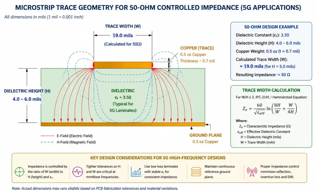
Controlled impedance routing: For 5G applications, single-ended traces are typically designed to 50 ohms, while differential pairs (used for high-speed digital interfaces like Ethernet backhaul) target 85, 90, or 100 ohms depending on the standard. At mmWave frequencies, even a 5% impedance variation can cause measurable signal degradation. This requires accurate control of trace width, dielectric thickness, and copper weight.
For a microstrip trace on a 5-mil dielectric with Dk of 3.5, achieving 50 ohms requires a trace width of approximately 10 mils. However, this calculation assumes no manufacturing variation. In practice, you must work with your PCB fabricator to characterize their process variation and design for the center of their capability window.
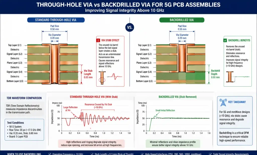
Via design and backdrilling: Through-hole vias act as stubs at high frequencies, creating resonances that degrade signal integrity. For signals above 10 GHz, via stubs longer than 15 mils typically require backdrilling to remove the unused portion of the via barrel. Blind and buried vias reduce stub length but increase cost. For massive MIMO designs where hundreds of RF channels must be routed, a hybrid approach using microvias for critical RF paths and backdrilled through-vias for lower-frequency signals offers the best cost-performance balance.
The via pad and anti-pad sizes also require careful optimization. Standard via pad sizes can create capacitive discontinuities that cause impedance dips. For 50-ohm traces, via pads should be minimized while still meeting IPC-6012 annular ring requirements (2 mils for Class 2, 4 mils for Class 3).
Trace roughness: Copper surface roughness increases loss at high frequencies due to the skin effect. Standard ED (electrodeposited) copper with 5-7 micron roughness can add 0.3 dB/inch loss at 28 GHz. Low-profile copper (RTF, HVLP, or VLP) with roughness under 2 microns reduces this loss by 30-40%. The additional cost of low-profile copper is justified for FR2 applications but may not be necessary for sub-6 GHz designs.
Here’s a design rule comparison for different 5G application scenarios:
| Design Parameter | Small Cell (FR1) | Macro Base Station (FR1) | mmWave Remote Radio Head (FR2) |
|---|---|---|---|
| Trace width (signal) | 4-6 mil | 5-8 mil | 3-5 mil |
| Trace spacing | 4 mil | 5 mil | 3 mil |
| Minimum via diameter | 8 mil | 10 mil | 6 mil (laser-drilled) |
| Via aspect ratio (max) | 12:1 | 10:1 | 8:1 |
| Annular ring (internal) | 2 mil | 3 mil | 2 mil |
| Impedance tolerance | ±7% | ±8% | ±5% |
| Copper roughness | Standard ED | Standard ED | VLP or RTF |
| Surface finish | ENIG | ENIG or Immersion Silver | ENIG (gold thickness 3-5 μin) |
These parameters reflect real-world manufacturing capability at leading PCB fabricators specializing in RF and microwave designs. Achieving tighter tolerances is possible but may require qualification of specialized suppliers and higher cost.
3. Material Selection for High-Frequency Performance
Material selection is the single most important decision for 5G PCB performance. The dielectric constant (Dk) and loss tangent (Df) directly determine signal loss, while coefficient of thermal expansion (CTE) affects reliability through thermal cycling.
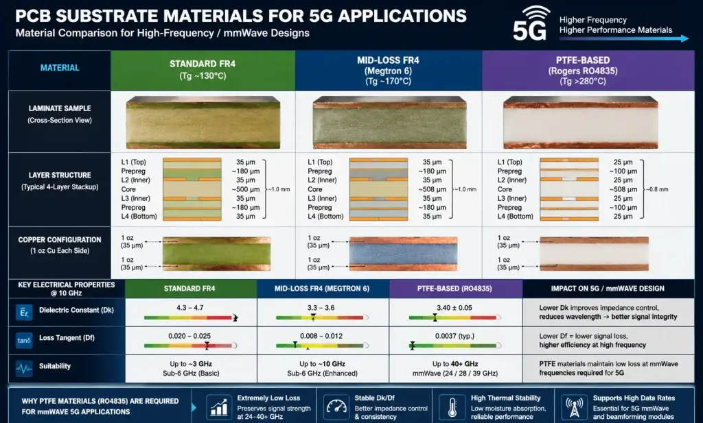
FR4 variants for sub-6 GHz: Standard FR4 with Dk of 4.2-4.5 and Df of 0.018-0.025 is acceptable for frequencies up to about 2 GHz but shows excessive loss for 5G FR1 applications. Mid-loss FR4 materials like Panasonic Megtron 6, Isola I-Speed, or Shengyi S7136H offer Df in the range of 0.008-0.012 at 10 GHz. These materials maintain FR4-like processing characteristics while delivering acceptable loss for sub-6 GHz 5G designs.
The cost premium for mid-loss FR4 over standard FR4 is typically 15-25%, which is far less than the cost of moving to PTFE-based materials. For base station designs operating primarily in the 3.5 GHz band, mid-loss FR4 represents the optimal cost-performance trade-off.
PTFE-based materials for mmWave: At frequencies above 20 GHz, PTFE-based laminates become necessary. Rogers RO4835 (Dk 3.48, Df 0.0037 at 10 GHz) and Taconic RF-35 (Dk 3.5, Df 0.0018 at 10 GHz) are common choices for 5G FR2 designs. These materials maintain low and stable Dk across temperature and frequency, which is essential for maintaining impedance control in outdoor deployments where temperature can vary from -40°C to +85°C.
The challenge with PTFE materials is manufacturability. They require specialized drilling parameters, longer cure cycles, and different via treatment compared to FR4. Not all PCB fabricators have qualified processes for PTFE laminates. When selecting a material, verify that your intended fabricator has experience with that specific material system.
Hybrid stackups: Cost optimization often drives hybrid stackup designs where PTFE is used only for the outer layers carrying mmWave signals, while the inner layers use mid-loss FR4 for power, ground, and lower-frequency digital signals. This requires careful management of CTE mismatch between material types. The bondply selection and press cycle must be optimized to avoid delamination.
The following table compares material properties for common 5G PCB laminates:
| Material | Supplier | Dk @ 10 GHz | Df @ 10 GHz | Tg (°C) | CTE-z (ppm/°C) | Typical Use Case |
|---|---|---|---|---|---|---|
| Standard FR4 | Various | 4.2-4.5 | 0.020 | 130-140 | 50-70 | Not recommended for 5G |
| Panasonic Megtron 6 | Panasonic | 3.6 | 0.008 | 180 | 45 | FR1 base stations, small cells |
| Isola I-Speed | Isola | 3.4 | 0.009 | 180 | 40 | FR1 remote radio heads |
| Shengyi S7136H | Shengyi | 3.5 | 0.010 | 170 | 48 | Cost-optimized FR1 |
| Rogers RO4835 | Rogers | 3.48 | 0.0037 | 280 | 32 | FR2 mmWave, hybrid stackup |
| Taconic RF-35 | Taconic | 3.5 | 0.0018 | 260 | 24 | FR2 critical RF layers |
| Rogers RO4003C | Rogers | 3.38 | 0.0027 | >280 | 46 | FR1 high-reliability |
Material selection must balance electrical performance, thermal reliability, and manufacturing cost. For prototype builds, Rogers materials offer the most predictable results due to widespread fabricator experience. For volume production, qualifying alternative materials like Taconic or Asian suppliers can reduce material cost by 20-30% without sacrificing performance.
4. Multilayer Stackup Design for 5G Applications
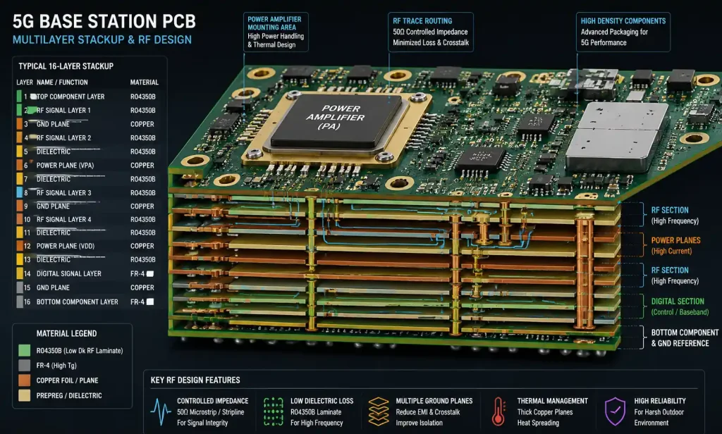
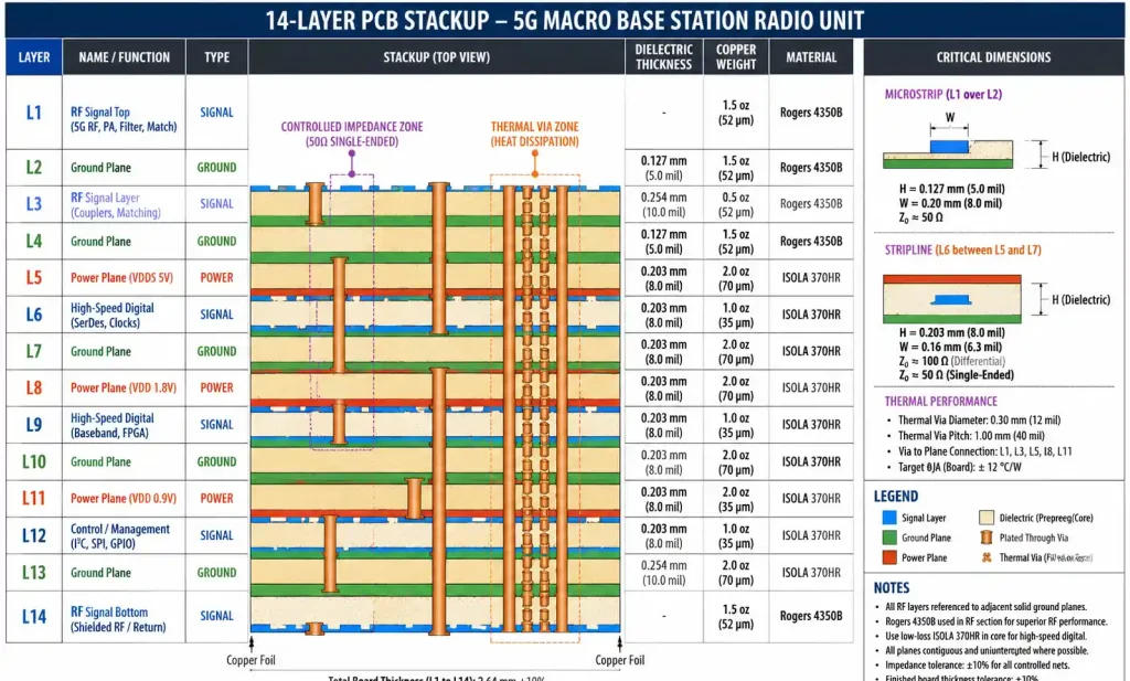
Stackup design for 5G telecommunication PCBs must simultaneously optimize for impedance control, signal isolation, thermal management, and EMI shielding. A typical base station radio unit requires 12-16 layers to accommodate RF signal routing, high-speed digital interfaces, and power delivery.
Layer allocation strategy: RF signal layers should be routed on outer layers or on layers immediately adjacent to ground planes. This provides the most controlled impedance environment and simplifies impedance calculation. High-speed digital signals (PCIe, Ethernet backhaul, CPRI/eCPRI) should be routed on inner stripline layers for better EMI containment. Power and ground planes should be interleaved to minimize PDN impedance.
A typical 14-layer stackup for a 5G macro base station radio unit might allocate layers as follows: L1 (RF TX/RX traces), L2 (ground), L3 (high-speed digital), L4 (power), L5 (ground), L6 (digital signals), L7 (power), L8 (ground), L9 (digital signals), L10 (power), L11 (ground), L12 (high-speed digital), L13 (ground), L14 (RF TX/RX traces).
Dielectric thickness selection: For 50-ohm microstrip on outer layers, typical dielectric thickness is 4-6 mils depending on the material Dk. Thinner dielectrics yield narrower traces for a given impedance, which can help with dense routing but make manufacturing more sensitive to process variation. For critical RF paths, a 5-mil dielectric with ±0.5 mil tolerance is a practical target for IPC Class 2 builds.
For inner stripline layers, the dielectric thickness above and below the trace should be symmetric to center the field. Asymmetric stripline creates odd-mode resonances that degrade signal quality. In practice, achieving perfect symmetry is difficult due to prepreg flow variation during lamination, so designing for 10-15% asymmetry tolerance is prudent.
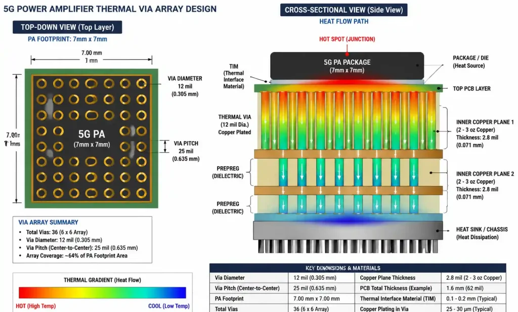
Thermal vias for power amplifiers: 5G power amplifiers (PAs) can dissipate 30-50 watts in a package smaller than 10mm x 10mm. Thermal vias directly under the PA thermal pad provide the primary heat extraction path. Via arrays should use 10-12 mil diameter vias on 20-25 mil pitch, with all vias connecting to internal copper planes that spread heat. For very high power designs, metal-core PCBs with aluminum substrates may be required.
The table below shows recommended stackup configurations for different 5G equipment types:
| Equipment Type | Layer Count | Outer Layer Material | Inner Layer Material | Total Thickness (mm) | Copper Weight (oz) |
|---|---|---|---|---|---|
| Small cell (FR1) | 10-12 | Mid-loss FR4 | Standard FR4 | 1.6 | Signal: 0.5, Power: 2 |
| Macro RRU (FR1) | 12-16 | Mid-loss FR4 | Standard FR4 | 2.0-2.4 | Signal: 0.5, Power: 2-3 |
| mmWave RRU (FR2) | 14-18 | Rogers RO4835 | Mid-loss FR4 | 2.0-2.8 | Signal: 0.5, Power: 2 |
| Massive MIMO (FR1) | 16-20 | Mid-loss FR4 | Standard FR4 | 2.8-3.2 | Signal: 0.5, Power: 3-4 |
| mmWave MIMO (FR2) | 18-24 | Rogers RO4835 | Mid-loss FR4/RO4350B | 3.0-3.6 | Signal: 0.25-0.5, Power: 3-4 |
These configurations represent field-proven designs from deployed 5G infrastructure. Actual layer count and thickness depend on component density, power requirements, and mechanical constraints of the enclosure.
5. DFM Considerations for Telecommunication PCB Assembly
Design for manufacturability (DFM) is critical for 5G telecommunication PCBs due to the tight tolerances required for high-frequency performance and the high cost of respins in base station equipment.
Impedance tolerance and testing: Controlled impedance is not optional for 5G designs. Every production panel should be tested using TDR (time-domain reflectometry) coupons. The coupon design should match the actual trace geometry used in the design, including the same layer, trace width, and adjacent copper distribution. Generic IPC-2141 coupons may not accurately represent your design’s impedance environment.
When specifying impedance tolerance, recognize that tighter tolerance costs more. For sub-6 GHz designs, ±7% tolerance (46.5-53.5 ohms for a 50-ohm trace) is achievable with standard process control. For mmWave, ±5% tolerance requires fabricator process characterization and may reduce panel yield by 5-10%, increasing cost.
Via reliability for thermal cycling: Telecommunication equipment experiences wide temperature swings in outdoor deployments. Thermal cycling between -40°C and +85°C creates stress on vias due to z-axis CTE mismatch between copper and dielectric. Via reliability is enhanced by using a minimum 2:1 pad-to-drill ratio, avoiding via-in-pad unless filled and plated over, and ensuring adequate copper plating thickness (minimum 1 mil for through-hole vias).
For high-power thermal vias, plating thickness should be increased to 1.2-1.5 mils to improve thermal conductivity and mechanical strength. Via filling with conductive epoxy further improves thermal performance but adds cost.
Solder mask and surface finish: ENIG (Electroless Nickel Immersion Gold) is the standard surface finish for 5G PCBs due to its flat surface (important for fine-pitch BGAs), excellent shelf life, and multiple reflow capability. Nickel thickness should be 3-5 microns, with gold thickness of 0.05-0.10 microns (2-4 microinches). Thicker nickel improves wear resistance for press-fit connectors but can create stress in fine-pitch pads.
Solder mask registration becomes critical for dense RF designs. Laser-defined solder mask (LDI) provides 1-mil registration accuracy compared to 2-3 mils for conventional photoimaging. For designs with 0.5mm pitch BGAs or dense via fields, LDI is worth the cost premium.
Common DFM issues in 5G telecommunication PCB assembly include:
| DFM Issue | Impact | Prevention Method | Cost of Fixing |
|---|---|---|---|
| Impedance out of spec | Signal integrity failure | TDR test coupons, process characterization | Full respin |
| Via breakout on inner layers | Reliability failure | Increase annular ring to 3+ mils | Full respin |
| Insufficient thermal relief | Solder joint voids | Thermal relief spokes on power planes | Rework possible |
| Solder mask slivers | Manufacturing defect/shorts | 4-mil minimum solder dam width | Yield loss 5-10% |
| Via stub resonance | Signal loss above 10 GHz | Backdrill vias or use blind vias | Full respin |
| Copper-to-board edge spacing | Routing damage during depanel | Maintain 20+ mil clearance | Panel yield loss |
These issues are best caught during a formal DFM review before sending Gerber files to fabrication. Most leading PCB suppliers offer free CAM review, but this typically only checks for manufacturing rule violations, not signal integrity or thermal performance issues. For high-value 5G designs, engaging an independent DFM consultant can prevent costly errors.
6. Thermal Management and Power Delivery
5G base stations and radio units generate significantly more heat than previous generations due to higher transmit power, increased processing requirements for massive MIMO beamforming, and higher power amplifier inefficiency at mmWave frequencies.
Power amplifier thermal design: A typical 5G macro base station radio unit contains 8-64 power amplifier chains, each dissipating 20-50 watts. The PA die junction temperature must remain below 125-150°C (depending on GaN or LDMOS technology) to ensure reliability. With ambient temperatures up to 55°C in outdoor deployments and case temperature potentially 20°C above ambient, the PCB thermal resistance becomes critical.
The primary heat path from PA package to heat sink is through thermal vias in the PCB. A typical thermal via array under a 7mm x 7mm PA package might include 30-40 vias of 12 mil diameter on 25 mil pitch. These vias must connect to thick copper planes (2-3 oz) that spread heat horizontally to reach the heat sink attachment points. Via fill with thermal epoxy (1-3 W/mK thermal conductivity) can improve thermal performance by 15-20% compared to air-filled vias.
Power delivery network design: 5G radio processing ASICs can draw peak currents of 30-50 amps with switching frequencies above 500 MHz. The PDN impedance must remain below 1-2 milliohms across the frequency range of interest to prevent voltage droop and noise coupling. This requires a combination of thick power planes (2-4 oz copper), high-capacitance plane spacing, and strategic placement of decoupling capacitors.
Plane capacitance is inversely proportional to plane spacing, so keeping power and ground planes close (4-6 mils) maximizes intrinsic capacitance. However, this must be balanced against the need for signal routing layers. A hybrid approach uses thin dielectric (4 mils) for power/ground plane pairs in the center of the stackup, while signal layers use thicker dielectric (5-8 mils) for easier impedance control.
Metal-core PCBs for extreme power: For outdoor radio units dissipating over 200 watts in a compact enclosure, standard FR4 PCBs may not provide sufficient thermal conductivity. Metal-core PCBs (MCPCBs) with aluminum or copper substrates offer thermal conductivity of 1-4 W/mK compared to 0.3 W/mK for FR4. The metal core is electrically isolated from copper traces by a thin dielectric layer (typically 3-6 mils).
MCPCBs are more expensive than standard PCBs and impose design constraints (typically only 1-2 copper layers, no through-vias), but they enable higher power density and can eliminate the need for additional heat spreaders. For 5G small cells designed for street furniture deployment, MCPCBs may be the only practical thermal solution.
Thermal management strategy comparison:
| Approach | Thermal Performance | Relative Cost | Best Application |
|---|---|---|---|
| Standard FR4 with thermal vias | Baseline | 1.0x | Low-power small cells (<50W) |
| Thick copper planes (3-4 oz) | +20-30% | 1.15x | Medium-power RRUs (50-150W) |
| Via fill with thermal epoxy | +15-20% | 1.10x | PA hotspots in standard designs |
| Metal-core PCB (1-2 layers) | +200-300% | 1.8-2.5x | High-power small cells, LED drivers |
| Hybrid metal-core/FR4 | +150-200% | 2.0-2.8x | Massive MIMO with mixed power zones |
| Vapor chamber integration | +300-400% | 3.0-4.0x | Extreme power density (>300W) |
The choice of thermal management approach depends on total power dissipation, enclosure size, ambient temperature range, and cost target. For outdoor macro base stations, active cooling (forced air or liquid) is typically used in combination with PCB thermal design, allowing standard thick-copper FR4 PCBs to handle the thermal load.
7. FAQ
What is the minimum layer count for a 5G base station PCB?
For sub-6 GHz (FR1) small cells, 10-12 layers is typical. Macro base stations and remote radio heads usually require 12-16 layers to accommodate RF routing, high-speed digital interfaces, and power delivery. mmWave (FR2) designs often use 14-20 layers due to the need for additional ground shielding and more complex antenna feed networks.
Can standard FR4 be used for 5G PCBs?
Standard FR4 with Df of 0.018-0.025 is generally not suitable for 5G due to excessive signal loss. For sub-6 GHz applications, mid-loss FR4 materials (Df 0.008-0.012) like Panasonic Megtron 6 or Isola I-Speed should be used. For mmWave applications above 20 GHz, PTFE-based materials like Rogers RO4835 are required to maintain acceptable loss.
What surface finish is recommended for 5G telecommunication PCBs?
ENIG (Electroless Nickel Immersion Gold) is the industry standard due to its flat surface, excellent shelf life, and multiple reflow capability. Nickel thickness should be 3-5 microns with gold thickness of 0.05-0.10 microns. Immersion silver is a lower-cost alternative for some applications but has shorter shelf life. OSP is not recommended for complex assemblies due to limited reflow cycles.
How do I calculate the impedance for a microstrip trace at 28 GHz?
Impedance calculation at mmWave frequencies requires field solver software (like Polar SI9000 or LineCalc) rather than simple equations, because dispersive effects and copper roughness significantly impact impedance. As a starting point, a 50-ohm microstrip on 5-mil RO4835 (Dk 3.48) requires approximately 11-mil trace width, but this must be verified with your fabricator’s process characterization data and adjusted for their copper weight and surface roughness.
Do all vias need to be backdrilled in 5G designs?
Backdrilling is required for signals above 10 GHz when through-hole vias are used and the stub length exceeds 15-20 mils. For sub-6 GHz designs, backdrilling is typically not necessary. Blind and buried vias eliminate stubs but increase cost by 40-60%. A hybrid approach using microvias for critical RF signals and standard vias for lower-frequency signals offers good cost-performance balance.
What is the typical impedance tolerance achievable for 5G PCBs?
For sub-6 GHz applications, ±7% impedance tolerance (46.5-53.5 ohms for a 50-ohm target) is achievable with standard fabrication process control. For mmWave applications, ±5% tolerance can be achieved but requires process characterization and may reduce panel yield. Tighter tolerances (±3%) are possible with specialized fabricators but at significantly higher cost.
How many thermal vias are needed under a 5G power amplifier?
For a typical 5G PA dissipating 30-50 watts in a 7mm x 7mm package, a thermal via array of 30-40 vias at 12-mil diameter on 25-mil pitch is typical. Vias should connect to 2-3 oz copper planes for heat spreading. Via fill with thermal epoxy improves performance by 15-20%. For very high-power PAs (>50W), metal-core PCBs may be required.
What is the lead time for 5G telecommunication PCB prototypes?
For mid-loss FR4 designs with controlled impedance, typical prototype lead time is 10-15 business days including impedance testing. Designs using Rogers or Taconic PTFE materials require 12-18 business days due to longer cure cycles and specialized processing. Hybrid stackups with mixed materials may require 15-20 business days. Expedited builds in 5-7 days are possible but at 2-3x normal cost.
8. Conclusion and Next Steps
Designing PCBs for 5G telecom infrastructure means juggling materials, controlled impedance, thermals, and what your fab can actually handle. Here’s the short version:For sub‑6 GHz (FR1): mid‑loss FR4 hits the sweet spot—good performance, easy to manufacture, and cost‑effective. Stick with standard impedance control ( ±7% tolerance is doable with a decent fab). Spend your real effort on PDN impedance and keeping power amps cool.
For mmWave (FR2) above 20 GHz: things get serious. You’ll need PTFE‑based materials, backdrill or blind vias to kill stubs, and tighten impedance tolerance to ±5%. Copper surface roughness matters now—use low‑profile foil. And not every fab can handle PTFE well, so talk to your supplier early.
Thermals are just as critical as signal integrity. A good via array under your PA can drop junction temperature by 20–30 °C. If you’re dissipating over 200 W, consider metal‑core or hybrid constructions.Before you send the design out, run a DFM check that covers impedance, thermal simulation, and manufacturing rules. Most 5G respins come from impedance drift or overheating—both predictable with proper simulation.
Working on a 5G design? Ask your fab for a free DFM review. Send them your stackup, target impedances, and thermal numbers upfront. For mmWave, partner with a specialized RF shop that has field solvers and process data—it’ll save you headaches and speed up deployment.