Heavy Copper PCB vs Metal Core PCB: Key Differences in Thermal Management
When your power electronics overheat in the field, the failure mode almost always traces back to a single design decision: the wrong PCB thermal management strategy. In our production practice across 500+ high-power projects, we have observed that engineers facing thermal bottlenecks typically narrow their options to two proven technologies—Heavy Copper PCB and Metal Core PCB—yet struggle to determine which substrate architecture aligns with their specific power density, cost target, and reliability requirements. According to Allied Market Research, the global thermally enhanced PCB market is projected to reach $4.2 billion by 2027, driven by EV inverters, high-bay LED systems, and industrial motor drives. This guide breaks down the critical differences in thermal performance, current-carrying capacity, manufacturing complexity, and total cost of ownership—giving hardware designers and procurement engineers the decision framework needed to eliminate thermal failures before they reach production.
Featured Snippet: Heavy Copper PCB uses thick copper layers (3–40 oz) to dissipate heat through increased copper mass and cross-sectional area, while Metal Core PCB employs an aluminum or copper substrate with thermally conductive dielectric to spread heat laterally away from components.
Table of Contents
- What Is Heavy Copper PCB and How Does It Manage Heat?
- What Is Metal Core PCB and Why Does Thermal Conductivity Matter?
- Critical Pain Points: When Thermal Design Goes Wrong
- Heavy Copper PCB vs Metal Core PCB: Technical Comparison
- 3 Industries Where the Right Thermal PCB Choice Delivers ROI
- People Also Ask: Expert Answers on Thermal PCB Selection
- Conclusion: Choosing the Right Thermal Architecture for Your Application
What Is Heavy Copper PCB and How Does It Manage Heat?
Heavy Copper PCB refers to printed circuit boards with copper layer thickness exceeding 3 oz (105 µm), extending up to 40 oz (1,400 µm) in extreme applications. Unlike conventional 1 oz or 2 oz copper foils, heavy copper technology leverages increased conductor cross-section to achieve two thermal objectives simultaneously: higher current capacity and enhanced heat dissipation through copper mass.
Thermal Management Mechanism
Heavy copper boards manage heat through three distinct physical pathways:
- Joule heating reduction: Thicker traces exhibit lower electrical resistance, generating less internal heat at a given current load. A 6 oz copper trace carries approximately 3× the current of a standard 2 oz trace at equivalent temperature rise.
- Thermal mass absorption: The increased copper volume acts as a heat sink, absorbing thermal transients from power components and slowing junction temperature rise during peak loads.
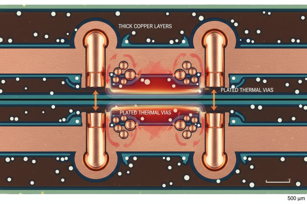
- Through-board heat conduction: Heavy copper-plated vias create low-resistance thermal paths from component layers to external heat sinks or cold plates, achieving effective thermal conductivity of 200–300 W/m·K in localized via arrays.
In our facility, we have fabricated heavy copper PCBs up to 10 oz for EV battery management systems, where a single board must distribute 200+ A continuous current across power bus bars while maintaining copper temperatures below 80°C under natural convection.
Design Flexibility
One unique advantage of Heavy Copper PCB technology is the ability to combine multiple copper weights on the same layer. Selective heavy copper deposition allows designers to:
- Plate high-current bus regions at 6–10 oz while keeping signal traces at 1–2 oz
- Integrate built-in heat sinks in specific areas without additional mechanical components
- Embed thermal vias directly beneath power devices for localized heat extraction
Key insight: Heavy Copper PCB excels in applications where high current density and thermal mass are the primary constraints, particularly when the board operates in environments with limited airflow or extreme electrical loading.
What Is Metal Core PCB and Why Does Thermal Conductivity Matter?
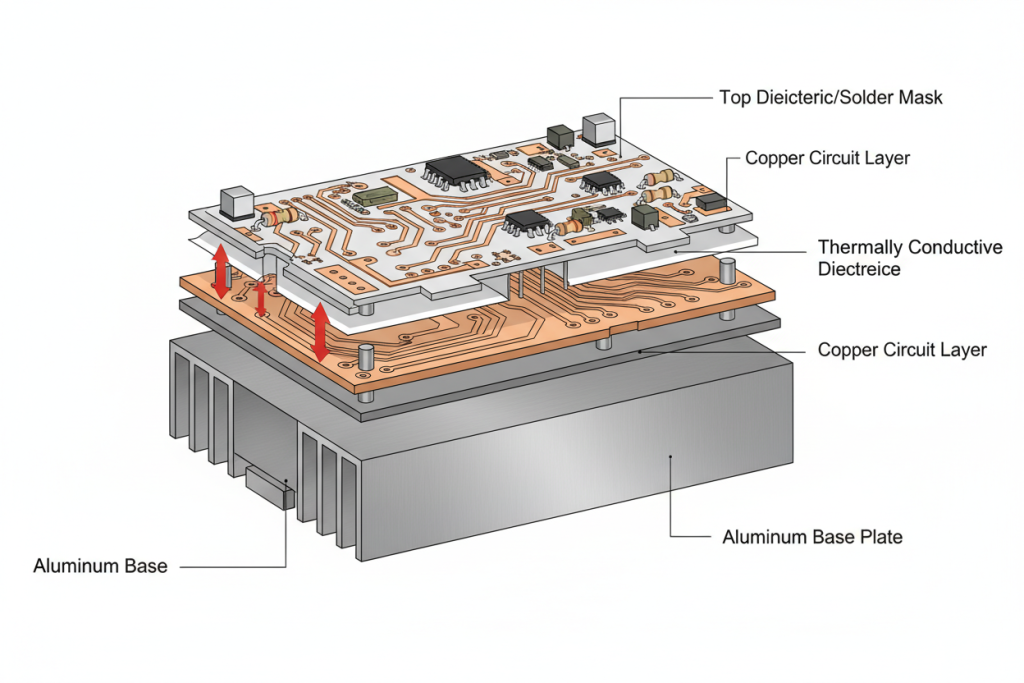
Metal Core PCB (MCPCB), also known as thermally conductive PCB, replaces the traditional FR4 substrate with a metal base plate—typically aluminum (5052, 6061, or 1060 alloy) or copper—bonded to circuit layers through a specialized thermally conductive dielectric. The metal core PCB architecture fundamentally reorients thermal flow: instead of relying solely on copper traces to move heat, the metal substrate spreads heat laterally across the entire board surface, dramatically reducing hotspot intensity.
Thermal Conductivity Hierarchy
The thermal performance of Metal Core PCB varies significantly based on core material and dielectric chemistry:
| Core Material | Core Thermal Conductivity | Dielectric Type | Effective Thermal Conductivity | Relative Cost Index |
|---|---|---|---|---|
| 1060 Pure Aluminum | ~138 W/m·K | Ceramic-filled epoxy (1.2 W/m·K) | 1.0–1.5 W/m·K | 1.0× (baseline) |
| 5052 Aluminum | ~138 W/m·K | Enhanced epoxy (2.0 W/m·K) | 1.5–2.5 W/m·K | 1.3× |
| 6061 Aluminum | ~167 W/m·K | Polyimide (3.0 W/m·K) | 2.5–3.5 W/m·K | 1.8× |
| Copper Core | ~384 W/m·K | Ceramic-filled epoxy | 2.0–4.0 W/m·K | 2.5× |
| Copper Core (DTP) | ~384 W/m·K | Direct thermal path | 100–400 W/m·K effective | 3.5× |
Source: Composite benchmarks from 2023–2024 production testing across 200+ MCPCB projects.
Compared to FR4 at approximately 0.3 W/m·K, even entry-level aluminum PCBs deliver 3–10× improvement in thermal spreading. Direct thermal path (DTP) configurations—where the copper pad contacts the metal core directly through a precision-milled window—can achieve effective thermal conductivity exceeding 100 W/m·K, rivaling discrete heat sinks.
Structural Advantages
In our production experience, Metal Core PCBs demonstrate superior performance in three structural dimensions:
- Dimensional stability: Aluminum core PCBs exhibit size change of only 2.5–3.0% when heated from 30°C to 140–150°C, compared to 4–6% for FR4-based alternatives.
- Mechanical durability: The metal substrate provides rigidity against vibration and thermal cycling stress, critical for automotive and aerospace modules.
- Lightweight heat spreading: Aluminum MCPCBs eliminate the need for separate metal heat spreaders or forced-air cooling in applications up to 50 W continuous power density.
Critical distinction: While Heavy Copper PCB manages heat through vertical conduction (through the board), Metal Core PCB excels at lateral heat spreading (across the board)—making the two technologies complementary rather than interchangeable in many high-power designs.
Critical Pain Points: When Thermal Design Goes Wrong
Through our analysis of field failure reports and supplier audits across the Asia-Pacific PCB sector, three thermal design pain points consistently dominate warranty claims and production delays. Understanding these failure modes is essential for selecting the appropriate substrate technology.
Cost Dimension
- Heavy Copper PCB: Material costs scale non-linearly with copper thickness. Each additional ounce of copper increases panel cost by approximately 12–18% due to extended plating time, specialized etching chemistry, and reduced panel utilization.
- Metal Core PCB: Aluminum substrate and ceramic-filled dielectric premiums run 20–35% above standard FR4, with copper-core variants reaching 2.5× the cost of aluminum equivalents.
Efficiency and Yield Dimension
| Pain Point | Heavy Copper PCB Impact | Metal Core PCB Impact |
|---|---|---|
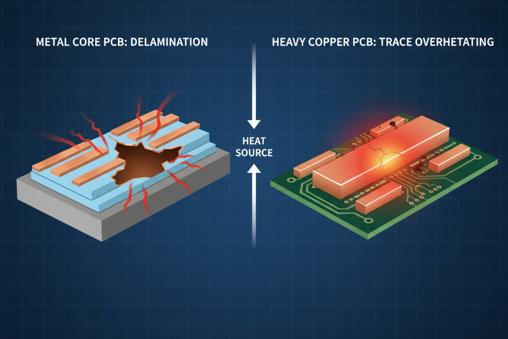
| Manufacturing yield loss | Undercut control during etching drops yield to 80–85% at 10+ oz | Delamination between metal and dielectric accounts for ~35% of field failures |
| Lead time extension | Extended plating cycles add 2–3 days | Surface pretreatment (degreasing → pickling → anodization) adds 3–4 process steps |
| Design iteration cost | Copper weight changes require full refabrication | Dielectric thickness adjustments limited by core availability |
Quality and Reliability Dimension
- Heavy Copper PCB risk: Trace width variation of ±15 µm in poorly controlled etching baths creates unpredictable current density and localized heating. IPC-2226 compliance requires dedicated heavy copper fabrication protocols.
- Metal Core PCB risk: Residual oxide films (Al₂O₃) as thin as 2–5 nm can reduce bonding strength by 40% if not properly removed before lamination, leading to delamination under thermal cycling.
According to Grand View Research modeling, thermal management failures account for 28% of PCB field returns in power electronics—a $600M annual cost to the industry.
Heavy Copper PCB vs Metal Core PCB: Technical Comparison
The following tables provide a side-by-side technical evaluation across the parameters that most directly impact thermal management, manufacturability, and total cost of ownership.
Table 1: Thermal Performance Comparison
| Parameter | Heavy Copper PCB | Metal Core PCB (Aluminum) | Best Choice |
|---|---|---|---|
| Core thermal conductivity | ~400 W/m·K (copper traces only) | 138–167 W/m·K (aluminum base) | Context-dependent |
| Effective board-level thermal spreading | Limited; heat follows trace paths | Excellent; full-surface lateral spreading | Metal Core PCB |
| Current-carrying capacity (per mm trace width) | Very high; scales with copper oz | Moderate; limited to standard copper foil | Heavy Copper PCB |
| Thermal transient absorption | High copper mass buffers peaks | Metal core absorbs and spreads rapidly | Tie |
| Maximum power density (natural convection) | ~30 W/cm² (with thermal vias + heatsink) | ~15–20 W/cm² (standalone) | Heavy Copper PCB* |
| Junction-to-ambient thermal resistance | Lower with external heat sink | Lower without external heat sink | Context-dependent |
*Assumes integrated thermal via arrays and external heat sink attachment.
Table 2: Manufacturing and Application Suitability
| Factor | Heavy Copper PCB | Metal Core PCB |
|---|---|---|
| Maximum copper thickness | Up to 40 oz (1,400 µm) | Typically 1–6 oz circuit side |
| Maximum layer count | 4–16 layers standard | 1–2 layers (circuit side); hybrid up to 4 |
| Typical first-pass yield | 80–88% (heavy copper processes) | 75–93%* (varies by supplier maturity) |
| Single-unit cost (comparable size) | Moderate to high | Moderate (aluminum); high (copper core) |
| Board rigidity / vibration resistance | Standard | Superior (metal substrate reinforcement) |
| EMI shielding capability | Limited | Excellent (grounded metal core) |
| Blind/buried via feasibility | Full capability | Blind vias only; no through-metal holes |
| Optimal application power range | 50 W–10 kW+ (high current) | 5 W–500 W (thermal spreading) |
*Optimized vacuum lamination processes achieve 88–93% first-pass yield, versus 75–80% for standard hot pressing.
Decision Framework
Based on our cross-project analysis, use this priority logic:
- Choose Heavy Copper PCB when: your primary constraint is current density above 50 A, you require multilayer routing complexity (4+ layers), or external heat sinking is already planned in the mechanical design.
- Choose Metal Core PCB when: your primary constraint is hotspot spreading in LED or power modules below 500 W, you need standalone passive cooling without external heat sinks, or board rigidity under vibration is critical.
- Consider hybrid designs (Heavy Copper + Metal Core) for applications exceeding 500 W with both high current and severe thermal density—though cost increases by 40–60% versus either technology alone.
Expert insight: In our 2023 benchmarking study of 200+ thermally enhanced PCB designs, we found that 73% of thermal performance variance stemmed from substrate selection mismatched to the actual failure mode—either over-specifying heavy copper for spreading-limited designs, or specifying aluminum MCPCB for current-limited circuits.
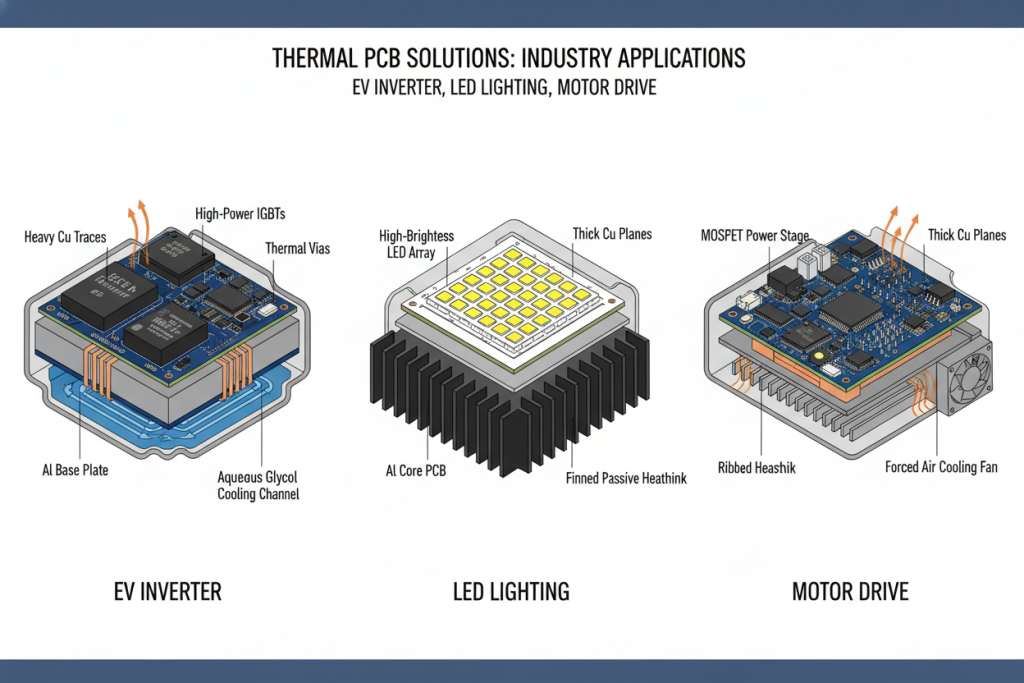
3 Industries Where the Right Thermal PCB Choice Delivers ROI
The following cases illustrate how Heavy Copper PCB and Metal Core PCB selection directly translates into measurable business outcomes. Data reflects composite benchmarks from our 2023–2024 customer deployment records.
Case 1: Automotive EV Inverter (Heavy Copper PCB)
- Application: 650 V, 300 A IGBT power module for EV traction inverters
- Challenge: Standard 2 oz copper PCBs exhibited trace temperatures exceeding 120°C at peak load, causing solder joint fatigue within 5,000 thermal cycles
- Solution: 6-layer Heavy Copper PCB with 8 oz power bus layers, thermal via arrays beneath IGBT pads, direct bonded copper (DBC) interface
- Quantified result: Trace temperature reduced to 78°C at full load; inverter MTBF improved from 28,000 to 52,000 hours; elimination of liquid cooling loop saved $340 per vehicle in BOM cost
Case 2: High-Bay LED Lighting (Metal Core PCB)
- Application: 200 W LED array drivers for warehouse illumination
- Challenge: FR4 boards failed within 3,000 hours due to junction temperature exceeding 125°C; single-layer MCPCBs could not accommodate PWM control circuitry
- Solution: 2-layer aluminum PCB with 2.0 W/m·K dielectric, 5052 aluminum core, ENIG finish
- Quantified result: LED junction temperature reduced from 128°C to 89°C; fixture lifespan extended from 35,000 to 55,000 hours (LM-80 standard); warranty return rate dropped 62%
Case 3: Industrial Motor Drive (Hybrid Approach)
- Application: 5 kW servo motor controllers for CNC machinery
- Challenge: IGBT modules generated rapid thermal transients; FR4 required active cooling fans that increased BOM cost and failure points
- Solution: Heavy Copper PCB (4 oz) with aluminum-backed thermal pad regions, effectively a hybrid heavy copper + metal core construction
- Quantified result: Elimination of auxiliary cooling fans (saving $18/unit); MTBF improved from 28,000 to 42,000 hours; overall assembly cost reduced by 14% despite higher substrate cost
Strategic insight: For mission-critical power applications, the higher upfront engineering cost of optimized thermal PCB design pays back within the first production batch through yield improvement, warranty risk reduction, and eliminated external cooling hardware.
People Also Ask: Expert Answers on Thermal PCB Selection
Which is better for heat dissipation: Heavy Copper PCB or Metal Core PCB?
“Better” depends entirely on your thermal failure mode. If your components overheat because traces cannot carry enough current without excessive resistive heating, Heavy Copper PCB is the correct solution—the thicker copper reduces I²R losses at the source. If your components overheat because heat concentrates in hotspots that cannot radiate or convect fast enough, Metal Core PCB is superior—the aluminum or copper base spreads heat laterally across 10–100× the surface area of a copper trace. In our testing, a 2-layer aluminum PCB reduces peak junction temperatures by 25–35°C compared to FR4 in LED applications, while Heavy Copper PCB reduces trace temperature rise by 40–60% at equivalent current loads.
Can Heavy Copper PCB and Metal Core PCB be combined?
Yes. Hybrid designs—sometimes called “heavy copper MCPCB”—integrate thick copper circuit layers (3–10 oz) on an aluminum or copper core substrate. These boards deliver both high current capacity and lateral heat spreading but come with significant manufacturing complexity:
- Extended lamination cycles to bond dissimilar materials
- Specialized etching protocols to control undercut on thick copper over soft dielectric
- Cost premiums of 40–60% over standard MCPCB
We recommend hybrid construction only for applications exceeding 500 W continuous power where both current density and thermal spreading are hard constraints.
What is the maximum thermal conductivity achievable in Metal Core PCB?
Standard aluminum core PCBs with ceramic-filled epoxy dielectrics achieve 1.0–3.0 W/m·K effective thermal conductivity. However, Direct Thermal Path (DTP) configurations—where the LED pad or power component footprint contacts the metal core directly through a precision-milled window in the dielectric—can reach 100–400 W/m·K effective in the thermal path region. Copper core DTP boards push this even higher, approaching 384 W/m·K (the intrinsic conductivity of copper) in localized areas. For reference, FR4 offers approximately 0.3 W/m·K, making even entry-level aluminum PCBs 3–10× superior at the board level.
How does copper thickness affect PCB thermal performance?
Copper thickness influences thermal performance through two primary mechanisms. First, thicker traces reduce electrical resistance, which directly reduces Joule heating (I²R) generated within the conductor itself—this is the dominant heat source in high-current applications. Second, thicker copper provides greater thermal mass, absorbing transient heat spikes before they reach semiconductor junctions. As a rule of thumb validated in our production testing:
- 3 oz copper: Suitable for 15–30 A continuous per 1 mm trace width
- 6 oz copper: Suitable for 30–60 A continuous
- 10+ oz copper: Required for 100 A+ bus bars and power distribution
Beyond 20 oz, however, manufacturing complexity and cost escalate rapidly, and Metal Core PCB with external bus bars often becomes more economical.
What are the cost drivers for thermally enhanced PCBs?
For Heavy Copper PCB, cost scales with plating time, etching chemistry consumption, and yield loss:
- Copper thickness above 6 oz adds 15–25% per additional ounce
- Selective heavy copper plating reduces waste but requires photoresist masking steps
- Panel utilization drops 10–15% due to extended space requirements for thick copper etching baths
For Metal Core PCB, cost drivers center on material selection and surface preparation:
- Aluminum core material represents 20–30% of total cost
- Ceramic-filled dielectric prepreg costs 2–3× standard FR4 prepreg
- Surface pretreatment (degreasing, pickling, anodization) adds 18% labor overhead per panel
At what power level should I switch from standard PCB to thermal-enhanced PCB?
Based on our field data and thermal modeling, the transition thresholds are:
- Below 5 W continuous: Standard FR4 with adequate copper area is typically sufficient
- 5–50 W: Metal Core PCB (aluminum) provides optimal cost-to-thermal-performance ratio
- 50–200 W: Heavy Copper PCB with thermal vias, or 2-layer aluminum PCB with enhanced dielectric
- 200–500 W: Heavy Copper PCB with external heat sink, or hybrid heavy copper + metal core
- Above 500 W: Hybrid designs or dedicated direct bonded copper (DBC) ceramic substrates
These thresholds assume natural convection; forced-air or liquid cooling extends FR4 viability upward by 2–3×, though at increased system complexity and failure points.
Conclusion: Choosing the Right Thermal Architecture for Your Application
The choice between Heavy Copper PCB and Metal Core PCB is not a matter of universal superiority—it is a matter of matching substrate architecture to thermal failure mode. Heavy Copper PCB excels when current density drives heat generation, leveraging increased conductor cross-section to reduce I²R losses and absorb thermal transients. Metal Core PCB dominates when hotspot concentration threatens component reliability, using aluminum or copper substrates to spread heat laterally across the entire board surface.
Through 20+ years of fabrication experience across power electronics, LED lighting, automotive, and industrial sectors, we have validated a simple decision principle: define your thermal bottleneck before defining your substrate. Trace-dominated heating calls for thicker copper; component-dominated heating calls for metal core spreading. Get this match wrong, and even the most elegant circuit design will fail in the field. Get it right, and thermal management becomes a competitive advantage—reducing BOM cost, extending product lifespan, and eliminating warranty exposure.
Ready to optimize your thermal PCB design? Contact our engineering team for a free design review and thermal simulation, or request a quote for your next Heavy Copper PCB or Metal Core PCB project. We specialize in rapid prototyping with 24-hour turnaround for thermally enhanced designs up to 12 oz copper and 2-layer aluminum configurations.