
How does wave soldering work? What is its process flow?
Wave soldering is a common electronic soldering process widely used in the electronics manufacturing industry. It can efficiently and quickly connect electronic components to printed circuit boards (PCBs). This article will introduce the working principle and process flow of wave soldering in detail to help readers understand the principle and operation process of wave soldering.
Working principle of wave soldering
Wave soldering uses surface tension and the characteristics of liquid solder to connect electronic components. Its working principle is as follows:
- Solder surge
In the wave soldering equipment, the solder (usually tin alloy) is heated to a liquid state and forms a solder wave with a bump. This solder wave is located on the pad and the shape of the wave is maintained by the agitator.
- Surface tension effect
The pins of the electronic components and the pads on the PCB will enter the solder wave after preheating. Due to the surface tension of the solder, the liquid solder will wrap the pin around to form a solder ball. At the same time, the solder will also cover the pad to form a welding area.
- Solder cooling
When the electronic components pass through the solder wave, the solder will cool down and solidify rapidly. During this process, the temperature of the solder wave gradually decreases, causing the solder to change from liquid to solid. The solidification of the solder makes the pins firmly connected to the pads.
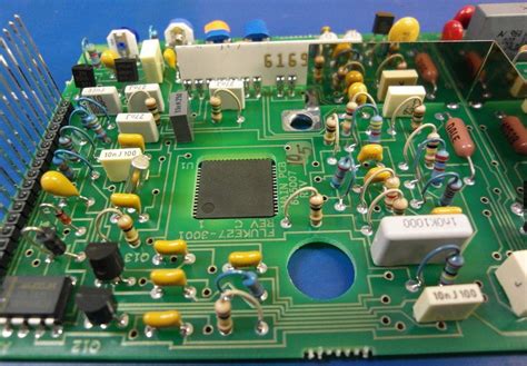
Wave soldering process
The wave soldering process includes the following key steps:
- PCB preparation
First, the PCB to be wave soldered needs to be prepared. This includes cleaning the PCB surface to ensure that there is no dirt and oxides, and setting the exact position of the pads.
- Component installation
Install electronic components on the PCB. This includes inserting the pins of the components into the corresponding pads. Before inserting the pins, the pins can be pretreated for electrostatic protection and heat resistance.
- Power transmission preheating
The PCB is sent into the wave soldering equipment with the installed electronic components. The equipment will use the preheating area to heat the PCB to ensure temperature control during the soldering process.
- Formation of tin wave crest
After the preheating area, the solder begins to melt and forms a solder wave crest. The melting temperature of the solder is set according to the specific welding requirements.
- Wave soldering
Through the transmission device, the PCB is slowly passed through the solder wave crest area. After the pin contacts the solder, the solder will surround the pin to form a solder ball and form a welding area on the pad. This process usually lasts for a few seconds.
- Cleaning and inspection
After completing wave soldering, the PCB needs to be cleaned and inspected. Cleaning can remove the residues and oxides generated during the soldering process. Inspection can ensure the quality of soldering and the good connection between the pin and the pad.
Wave soldering is a commonly used electronic assembly technology for connecting electronic components (such as resistors, capacitors, chips, etc.) to pads on printed circuit boards (PCBs). Its working principle and process flow are as follows:
- Principle:
Wave soldering uses molten solder to form a liquid wave crest, and then conveys the PCB along the wave crest direction so that the pad contacts the solder and forms a solder joint. Solder is usually a tin alloy, which is melted by heating and forms a wave crest by surface tension.
- Process flow:
a. Preparation: Prepare the PCB and the components to be soldered, and ensure that they are positioned correctly and without error.
b. Apply solder paste: Apply solder paste on the PCB pads. The solder paste usually contains an alloy with a suitable melting temperature and viscosity to enhance the solder joint connection.
c. Positioning components: Place the components to be soldered on the pads of the PCB, ensuring that the components are aligned with the pads.
d. Preheating: Preheat the PCB to remove moisture, volatile organic matter, etc.
e. Wave soldering: Move the PCB along the conveyor line of the wave soldering equipment so that the pads are in contact with the liquid solder. The solder wets and melts the solder paste on the pads and forms solder joints.
f. Cooling and solidification: After the solder joints are formed, the PCB continues to move along the conveyor line to the cooling area, and the solder joints are cooled and solidified.
The entire wave soldering process needs to control appropriate parameters such as temperature, time and speed to ensure the quality of solder joints and the reliability of component connections. In addition, attention should be paid to factors such as the quality of solder paste applied to the pads, the selection of solder and the debugging of wave soldering equipment to improve the soldering effect.
Wave soldering is an efficient and reliable electronic soldering process. It is based on the working principle of solder wave and surface tension, and can reliably connect electronic components to PCBs. The process of wave soldering includes key steps such as PCB preparation, component installation, preheating, soldering, cleaning and inspection. Proficiency in the principles and process of wave soldering can ensure soldering quality and improve manufacturing efficiency.