
How to Implement PCB Solder Mask Opening (SMO): A Comprehensive Guide
1. Introduction
Printed Circuit Boards (PCBs) are essential components in modern electronics, providing mechanical support and electrical connections for electronic components. One critical aspect of PCB design and manufacturing is the solder mask opening (SMO), also known as “PCB开窗” in Chinese. Solder mask openings are areas where the solder mask is removed to expose underlying copper pads, allowing for soldering, testing, or heat dissipation.
This article explores the methods, design considerations, and manufacturing processes involved in implementing PCB solder mask openings, ensuring reliable and high-quality PCB fabrication.
2. What is a PCB Solder Mask Opening?
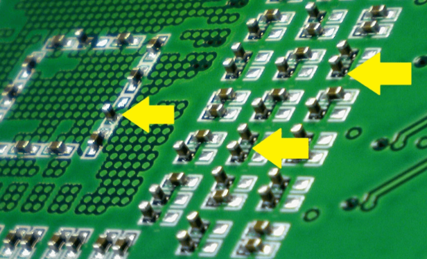
The solder mask is a protective layer applied over the copper traces of a PCB to prevent oxidation, short circuits, and solder bridging during assembly. However, certain areas must remain exposed for:
- Component soldering (pads for SMD or through-hole components)
- Test points (for debugging and validation)
- Heat dissipation (exposed copper for better thermal performance)
- High-current traces (to allow additional solder for increased conductivity)
A solder mask opening (SMO) is the intentional removal of the solder mask in these areas.
3. Methods to Implement PCB Solder Mask Openings
There are several ways to create solder mask openings in PCB manufacturing:
3.1. Design-Based Solder Mask Openings (Gerber Files)
The most common method is defining openings in the solder mask layer (Gerber file) during PCB design. Designers use CAD tools (e.g., Altium Designer, KiCad, Eagle) to specify openings by:
- Creating a solder mask layer that defines where openings should be.
- Adjusting solder mask expansion/contraction to control the opening size relative to the copper pad.
- Using different colors (e.g., green for mask, clear for openings).
Example in Altium Designer:
- Open the PCB design file.
- Navigate to the solder mask layer (Top/Bottom Solder).
- Draw shapes (pads, lines, polygons) where openings are needed.
- Ensure proper clearance from adjacent traces.
3.2. Manual Solder Mask Removal (Post-Processing)
In some cases, solder mask openings are created manually after PCB fabrication:
- Laser ablation: A laser removes the solder mask precisely.
- Mechanical scraping: A fine blade scrapes off the mask (less precise).
- Chemical etching: A solvent dissolves the mask in selected areas.
This method is useful for prototyping or modifications but is less precise than design-based openings.
3.3. Selective Solder Mask Application
Some manufacturers apply solder mask only where needed, leaving other areas exposed. This is common in:
- High-power PCBs (where large copper areas must remain exposed).
- RF/microwave PCBs (to minimize dielectric interference).
4. Design Considerations for Solder Mask Openings
To ensure proper functionality, consider the following:
4.1. Solder Mask Expansion/Contraction
- Standard expansion: Typically 0.05mm–0.1mm larger than the pad to prevent misalignment.
- Tented vias: Vias covered with solder mask to prevent solder wicking.
- Non-solderable areas: Ensure critical traces remain masked to avoid shorts.
4.2. Copper Pad Size vs. Solder Mask Opening
- If the opening is too large, solder may spread excessively.
- If the opening is too small, solderability decreases.
4.3. Thermal Relief for Large Copper Areas
- For thermal pads (e.g., QFN/DFN packages), use thermal spokes to balance heat dissipation and soldering.
4.4. Solder Mask Material and Thickness
- LPI (Liquid Photoimageable Solder Mask): Most common, high precision.
- Dry Film Solder Mask: Used in HDI PCBs.
- Thickness: Typically 10–25µm after curing.

5. PCB Manufacturing Process for Solder Mask Openings
The standard process involves:
- PCB Cleaning – Remove oxidation and debris.
- Solder Mask Application – Spray, curtain coat, or screen-print.
- Pre-Baking – Partially cure the mask.
- UV Exposure – Use a photomask (from Gerber files) to define openings.
- Development – Wash away unexposed mask, revealing openings.
- Final Curing – Fully harden the solder mask.
6. Common Issues & Solutions
| Issue | Cause | Solution |
|---|---|---|
| Solder mask bleeding | Overexposure/underexposure | Adjust UV exposure time |
| Incomplete openings | Poor development | Increase developer solution strength |
| Misaligned openings | Registration errors | Improve alignment marks |
| Solder mask peeling | Poor adhesion | Ensure proper surface cleaning |
7. Applications of PCB Solder Mask Openings
- SMD Assembly: Exposed pads for reflow soldering.
- Test Points: Allows probe contact for debugging.
- High-Power Electronics: Exposed copper for heat dissipation.
- EMI Shielding: Ground pads for shielding cans.
8. Conclusion
Implementing PCB solder mask openings requires careful design and manufacturing control. By defining openings in Gerber files, selecting the right solder mask material, and following best practices, engineers can ensure reliable soldering, testing, and thermal performance. Whether for prototyping or mass production, understanding SMO techniques is crucial for high-quality PCB fabrication.
For further optimization, consult your PCB manufacturer regarding their solder mask capabilities and design rules. Proper implementation will enhance both functionality and manufacturability.