
Utilizing PCB Layout Techniques for RF Noise Suppression in Audio Amplifiers
Abstract
Radio Frequency (RF) noise interference is a critical challenge in audio amplifier design, often leading to degraded signal integrity, audible distortions, and electromagnetic compatibility (EMC) issues. This paper explores effective Printed Circuit Board (PCB) layout techniques to mitigate RF noise in audio amplifiers. Key strategies include proper grounding schemes, component placement, trace routing, shielding, and the use of filtering components. By implementing these techniques, designers can significantly reduce RF-induced noise and improve the overall performance of audio amplification systems.
1. Introduction
Audio amplifiers are susceptible to RF interference, especially in environments with strong electromagnetic fields, such as wireless communication devices, switching power supplies, and digital circuits. RF noise can couple into audio circuits through conduction, radiation, or parasitic elements, resulting in unwanted hum, hiss, or oscillations. Since traditional filtering methods alone may not suffice, optimizing the PCB layout is essential for minimizing RF interference.
This paper discusses practical PCB design approaches to enhance RF noise immunity in audio amplifiers, covering:
- Grounding strategies (star grounding, split planes, and avoiding ground loops)
- Component placement and routing techniques
- Shielding and filtering methods
- Parasitic capacitance and inductance minimization
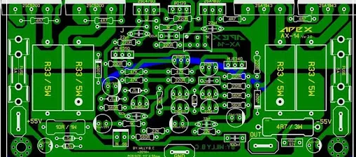
2. RF Noise Coupling Mechanisms in Audio Amplifiers
RF noise can infiltrate audio circuits through several pathways:
2.1 Conducted Noise
- Enters via power supply lines, input/output cables, or poorly filtered connections.
- High-frequency noise from switching regulators or digital circuits can couple into analog audio paths.
2.2 Radiated Noise
- Electromagnetic fields from nearby RF sources (e.g., Wi-Fi, Bluetooth, or cellular signals) induce currents in amplifier traces.
- Loop antennas formed by long PCB traces or unshielded wiring can pick up interference.
2.3 Parasitic Coupling
- Stray capacitance and inductance between traces or components can transfer RF energy.
- Poorly designed return paths create ground loops, exacerbating noise issues.
3. PCB Layout Techniques for RF Noise Suppression
3.1 Proper Grounding Techniques
3.1.1 Star Grounding
- Centralize the ground connection at a single point to prevent ground loops.
- Separate analog and digital ground planes, connecting them at one location.
3.1.2 Ground Plane Design
- Use a continuous ground plane to provide low-impedance return paths.
- Avoid splits in the ground plane beneath sensitive analog components.
3.2 Component Placement and Routing
3.2.1 Critical Signal Paths
- Keep input traces short and away from high-frequency components.
- Route audio signals differentially (if applicable) to reject common-mode noise.
3.2.2 Power Supply Decoupling
- Place decoupling capacitors (e.g., 100nF ceramic + 10μF electrolytic) close to IC power pins.
- Use multiple vias to connect decoupling capacitors to the ground plane.
3.2.3 High-Frequency Component Isolation
- Separate RF/noisy components (e.g., switching regulators, microcontrollers) from analog audio sections.
- Use guard rings or moats to isolate sensitive circuits.
3.3 Shielding and Filtering
3.3.1 EMI Shielding
- Enclose RF-prone sections in a shielded can or use copper pour as a shield.
- Implement grounded copper fences around high-frequency traces.
3.3.2 Filter Components
- Use ferrite beads or LC filters on power and signal lines.
- Implement RF chokes at amplifier inputs to block high-frequency interference.
3.4 Minimizing Parasitics
- Reduce trace lengths to minimize parasitic inductance.
- Avoid parallel routing of high-speed and audio signals to prevent capacitive coupling.
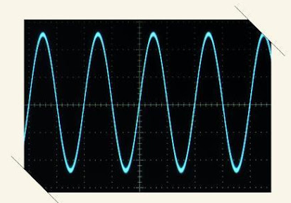
4. Case Study: RF Noise Reduction in a Class-D Audio Amplifier
A Class-D amplifier with PWM switching frequencies in the MHz range was experiencing RF noise interference. By applying the following PCB techniques, noise was reduced by >20dB:
- Revised Grounding: Implemented a star ground with separate analog/digital planes.
- Improved Decoupling: Added low-ESR capacitors near the switching MOSFETs.
- Shielding: Used a copper pour under the inductor to contain magnetic fields.
5. Conclusion
Effective PCB layout design is crucial for suppressing RF noise in audio amplifiers. By optimizing grounding, component placement, shielding, and filtering, designers can significantly enhance signal integrity and EMC performance. Future work may explore advanced materials (e.g., high-permeability substrates) for further noise reduction.