
How to Use Return Paths for Better PCB Design
Introduction
Printed Circuit Board (PCB) design is a complex process that involves careful consideration of signal integrity, power distribution, and electromagnetic compatibility (EMC). One of the most critical yet often overlooked aspects of PCB design is the return path—the path that current takes to return to its source. A poorly designed return path can lead to signal integrity issues, increased electromagnetic interference (EMI), and degraded performance.
This article explores the importance of return paths in PCB design, common challenges, and best practices for optimizing return paths to achieve better signal integrity, reduced noise, and improved EMC performance.
Understanding Return Paths
What Is a Return Path?
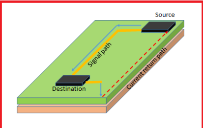
In any electrical circuit, current flows in a loop: from the source, through the signal trace, and back to the source through a return path. In DC circuits, the return path is straightforward—usually through a ground plane. However, in high-frequency AC circuits, the return current follows the path of least impedance, which is typically directly beneath the signal trace on an adjacent reference plane (ground or power).
Why Is the Return Path Important?
- Signal Integrity – A well-defined return path minimizes loop inductance, reducing signal distortion and reflections.
- EMI Reduction – A controlled return path prevents high-frequency currents from radiating noise.
- Power Integrity – A low-impedance return path ensures stable power delivery to components.
If the return path is disrupted (e.g., by splits in the ground plane or improper via placement), the current will find an alternative path, often increasing loop area and leading to EMI and signal degradation.
Common Return Path Issues in PCB Design
1. Split Planes and Gaps in Ground
When a signal trace crosses a split in the ground plane, the return current is forced to take a longer detour, increasing loop inductance and EMI.
2. Improper Via Transitions
If a signal changes layers without providing a nearby return via, the return current must find an alternative path, increasing loop area and noise.
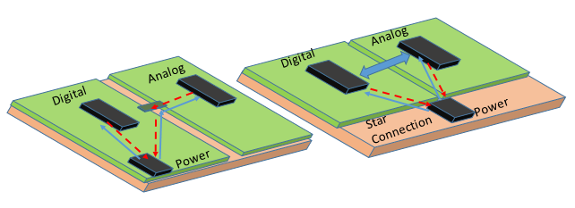
3. Mixed Signal Layouts (Digital & Analog)
Poor separation of digital and analog grounds can lead to noise coupling through return paths.
4. High-Speed Signals Without Reference Planes
High-speed signals (e.g., DDR, USB, PCIe) require an uninterrupted reference plane beneath them to maintain controlled impedance and minimize crosstalk.
Best Practices for Optimizing Return Paths
1. Use Continuous Ground Planes
- Avoid splitting ground planes unnecessarily.
- If splits are required (e.g., for isolation), ensure signals do not cross them.
- Use stitching capacitors to bridge ground planes when necessary.
2. Provide Return Vias for Layer Transitions
- When a signal changes layers, place a return via adjacent to the signal via to maintain a low-impedance return path.
- Follow the “1:1 via rule”—for every signal via, provide a nearby ground via.
3. Control Impedance with Proper Reference Planes
- Ensure high-speed signals have an unbroken reference plane (ground or power).
- Use microstrip or stripline configurations for controlled impedance traces.
4. Manage Mixed-Signal Return Paths
- Use a single ground plane for mixed-signal designs (instead of splitting analog and digital grounds).
- Partition noisy and sensitive circuits spatially rather than splitting the ground.
5. Minimize Loop Area
- Keep signal traces and their return paths as close as possible.
- Avoid large loops by ensuring the return current flows directly beneath the signal trace.
6. Use Decoupling Capacitors Effectively
- Place decoupling capacitors near IC power pins to provide a low-impedance return path for high-frequency noise.
Advanced Techniques for High-Speed Designs
1. Return Path Analysis in Simulation
- Use PCB simulation tools (e.g., HyperLynx, SIwave) to analyze return current distribution.
- Identify discontinuities in return paths before fabrication.
2. Differential Pair Routing
- Ensure differential pairs have symmetric return paths to maintain balance and reduce common-mode noise.
3. Power-Aware Return Path Design
- Recognize that high-speed signals may use power planes as return paths (due to capacitive coupling).
- Ensure proper decoupling to maintain low impedance across power planes.
Conclusion
A well-designed return path is essential for high-performance PCB designs, particularly in high-speed and mixed-signal applications. By following best practices—such as maintaining continuous reference planes, minimizing loop area, and providing proper return vias—designers can significantly improve signal integrity, reduce EMI, and enhance overall circuit reliability.
Advanced techniques, including simulation and careful power/ground planning, further optimize return paths in complex designs. By prioritizing return path integrity, PCB designers can avoid common pitfalls and achieve better-performing electronic systems.
Key Takeaways:
- Always provide a low-impedance return path for high-frequency signals.
- Avoid splits in reference planes where critical signals are routed.
- Use return vias when signals transition between layers.
- Simulate return paths in high-speed designs to preempt EMI issues.
By implementing these strategies, engineers can ensure robust, noise-resistant PCB designs that meet modern performance demands.
This article provides a comprehensive overview of return path optimization in PCB design. Would you like any sections expanded or additional details on specific topics?