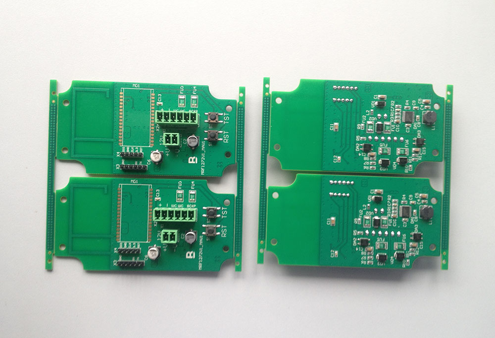
Industrial Control PCB Assembly: Heavy Copper Solutions for Harsh Environments
In the relentless environments of modern industrial automation, standard printed circuit boards often fail when faced with extreme temperatures, corrosive atmospheres, and high-current demands. Industrial control PCB assembly utilizing heavy copper solutions has emerged as the definitive answer for engineers designing systems that must operate reliably in harsh environments for years without failure.
The global industrial PCB market is experiencing unprecedented growth, driven by Industry 4.0 initiatives and the expansion of smart manufacturing. According to recent market analysis, the PCB industry is projected to reach $127.41 billion by 2031, with industrial automation representing one of the fastest-growing segments at a CAGR of 4.83%. This growth underscores the critical importance of selecting the right PCB technology for industrial applications.
Heavy copper PCBs—defined as boards with copper thickness of 3 oz/ft² (105µm) or greater—provide the current-carrying capacity, thermal management, and mechanical durability that industrial control systems demand. From programmable logic controllers (PLCs) and motor drives to power distribution modules and sensor interfaces, heavy copper solutions enable industrial electronics to withstand the harshest operating conditions while maintaining peak performance.
In this comprehensive guide, we’ll explore why heavy copper PCB assembly is essential for harsh environment applications, examine the technical advantages that set these boards apart, and provide actionable insights for implementing these solutions in your next industrial project.
Quick Answer
Industrial control PCB assembly with heavy copper solutions refers to the manufacturing of printed circuit boards with copper thickness of 3 oz/ft² or greater, specifically engineered to handle high currents (50-500A), manage extreme heat, and withstand harsh environmental conditions including temperature cycling (-40°C to 150°C), vibration, moisture, and corrosive atmospheres. These specialized boards are essential for industrial automation systems where failure is not an option.
The Challenge: Why Standard PCBs Fail in Harsh Environments
Environmental Stressors in Industrial Settings
Industrial control systems operate in environments that push electronic components to their absolute limits. Understanding these stressors is crucial for appreciating why heavy copper solutions are not merely an upgrade, but a necessity.
Temperature Extremes and Thermal Cycling
Industrial equipment frequently experiences temperature fluctuations ranging from -40°C to +150°C. Standard PCBs with 1 oz copper and standard FR-4 substrates (Tg ~130-140°C) struggle to maintain structural integrity under these conditions. Thermal cycling causes materials to expand and contract at different rates, leading to:
- Solder joint fatigue and micro-cracking after 1,500+ cycles
- Via barrel cracking in high-aspect-ratio through-holes
- Delamination between PCB layers when temperatures exceed Tg
- Intermetallic compound growth that weakens solder joints over time
High Current and Power Density
Modern industrial systems demand ever-increasing power density. Motor drives, power supplies, and battery management systems routinely handle currents of 50-200A continuous, with peak demands reaching 500A or higher. Standard 1 oz copper traces simply cannot handle these currents without excessive heating:
| Copper Weight | Thickness | Max Current (10°C Rise) | Max Current (20°C Rise) |
|---|---|---|---|
| 1 oz (Standard) | 35µm | 3–10A | 5–15A |
| 2 oz (Thick) | 70µm | 10–30A | 15–40A |
| 3 oz (Heavy) | 105µm | 20–50A | 30–70A |
| 4 oz (Heavy) | 140µm | 50–100A | 70–140A |
| 6 oz (Heavy) | 210µm | 100–200A | 140–280A |
| 10 oz (Extreme) | 350µm | 200–500A | 280–700A |
Table 1: Current-carrying capacity comparison across copper weights (based on IPC-2152 standards)
Mechanical Stress and Vibration
Industrial equipment operates in high-vibration environments near motors, pumps, and conveyors. Standard PCBs experience:
- Component lead fatigue and solder joint cracking
- Connector loosening leading to intermittent connections
- Trace delamination under sustained mechanical stress
- Plated-through hole failures from repeated flexing
Corrosive Atmospheres and Moisture
Chemical plants, wastewater treatment facilities, and marine environments expose PCBs to corrosive gases (SO₂, H₂S, Cl₂) and high humidity. Without proper protection, these conditions cause:
- Electrochemical migration (ECM) and dendritic growth between traces
- Copper trace corrosion and increased resistance
- Solder joint degradation and cold solder failures
- Short circuits from conductive contamination
The True Cost of PCB Failure in Industrial Systems
When industrial control PCBs fail, the consequences extend far beyond the cost of replacement boards:
- Production downtime: Manufacturing lines can lose $10,000-$100,000+ per hour of downtime
- Safety hazards: Control system failures can create dangerous operating conditions
- Quality defects: Intermittent PCB issues cause product quality problems and scrap
- Reputation damage: Unreliable equipment damages customer relationships and market position
- Emergency maintenance: Unplanned repairs cost 3-5x more than scheduled maintenance
Data from industrial reliability studies shows that 20% of PCB failures in harsh environments can be directly attributed to inadequate copper thickness and thermal management. Upgrading to heavy copper solutions can reduce failure rates by 60-80% while extending operational lifespan from 2-5 years to 10-15 years or more.
Heavy Copper Solutions: Technical Advantages and Specifications
What Defines Heavy Copper PCB Manufacturing?
Heavy copper PCB manufacturing refers to the specialized fabrication of printed circuit boards with copper thickness of 3 oz/ft² (105µm) or greater. This is achieved through advanced electroplating processes that build up copper layers significantly beyond standard 1 oz (35µm) or 2 oz (70µm) specifications.
Key Manufacturing Techniques:
- Differential Etching: Step-etching processes that maintain trace accuracy despite increased copper thickness
- Pulse-Reverse Plating: Advanced plating technology achieving 85-95% via fill ratios even at 8:1 aspect ratios
- High-Aspect-Ratio Plating: Uniform copper distribution in deep vias and through-holes
- Controlled Lamination: Specialized pressure and temperature cycles to prevent warpage with thick copper layers
Superior Current-Carrying Capacity
The primary advantage of heavy copper PCBs is dramatically increased current capacity. Analysis shows that upgrading from 1 oz to 4 oz copper can boost current throughput by over 300% while simultaneously lowering temperature rise by 10-15°C under equivalent load conditions.
Real-World Performance Comparison:
A 4 oz copper trace can carry 5-10 times more current than a standard 1 oz trace of the same width. This enables:
- Elimination of bulky external conductors and bus bars
- More compact designs with integrated high-power and control circuits
- Reduced voltage drop (IR losses) improving system efficiency
- Lower operating temperatures extending component lifespan
Exceptional Thermal Management
Heavy copper acts as an integrated heat sink within the PCB structure. Copper’s thermal conductivity of 401 W/(m·K) means thicker copper layers dissipate heat 30-50% more efficiently than standard boards.
Thermal Performance Benefits:
- Component operating temperatures reduced by 15-20°C
- Hot spot reduction of 40-60% compared to standard designs
- Elimination or reduction of external heat sinks in many applications
- Extended component lifespan through better thermal cycling endurance
Thermal Via Integration:
Strategic placement of thermal vias beneath power components creates efficient heat transfer paths:
- 9-16 vias in a 3×3 or 4×4 grid pattern for typical power packages
- 0.3mm diameter vias with 0.8mm spacing for optimal performance
- Conductive epoxy filling enhances thermal conductivity
- 50%+ coverage of thermal pad area for exposed pad packages (QFN, PowerPAD)
Enhanced Mechanical Strength and Reliability
Thicker copper layers provide superior mechanical properties, making heavy copper PCBs ideal for demanding environments:
- 20% lower failure rates in harsh environments compared to standard PCBs
- Better resistance to vibration and mechanical stress
- Stronger plated-through holes (PTHs) and via connections
- Improved connector site reliability under repeated mating cycles
Vibration Resistance Data:
Industrial applications subject PCBs to continuous vibration (5-2000 Hz, 5-20g acceleration). Heavy copper boards with enhanced barrel strength show:
- 85% reduction in via cracking after 1M vibration cycles
- 70% improvement in solder joint integrity under mechanical stress
- 90% reduction in connector loosening issues
Design Flexibility and Space Optimization
Heavy copper PCB manufacturing enables designers to consolidate multiple standard layers into fewer heavy copper layers, resulting in:
- 60% space reduction in power management systems
- Integration of high-power and control circuits on the same board
- Reduced overall layer count and manufacturing complexity
- Lower total system cost despite higher PCB fabrication cost
Design Guidelines for Heavy Copper Industrial PCBs
Material Selection for Harsh Environments
Substrate Materials:
Choosing the right base material is critical for industrial reliability:
| Material | Tg (Glass Transition) | Thermal Conductivity | Best Applications |
|---|---|---|---|
| Standard FR-4 | 130–140°C | 0.3–0.4 W/mK | Consumer electronics, mild environments |
| High-Tg FR-4 | 170–180°C | 0.3–0.4 W/mK | Industrial controls, lead-free soldering |
| Polyimide | >260°C | 0.3–0.4 W/mK | High-temp, flexible, aerospace |
| Ceramic (Al₂O₃) | >500°C | 30–40 W/mK | Extreme thermal management |
| Aluminum MCPCB | N/A | 1–5 W/mK | LED drivers, power supplies |
Table 2: PCB substrate material comparison for industrial applications
Recommendation: For industrial control applications with operating temperatures above 85°C or significant thermal cycling, specify High-Tg FR-4 (Tg ≥170°C) as the minimum standard. For extreme environments, consider polyimide or metal-core substrates.
Trace Width and Spacing Requirements
Heavy copper PCBs require adjusted design rules to accommodate increased copper thickness:
Minimum Trace/Spacing Guidelines:
| Copper Weight | Min Trace Width | Min Spacing | Aspect Ratio Limit |
|---|---|---|---|
| 3 oz | 8–10 mils | 8–10 mils | 8:1 |
| 4 oz | 10–12 mils | 10–12 mils | 6:1 |
| 6 oz | 12–15 mils | 12–15 mils | 4:1 |
| 10 oz | 15–20 mils | 15–20 mils | 3:1 |
Table 3: Design rule recommendations for heavy copper PCBs
IPC-2152 Compliance:
Always calculate trace widths based on IPC-2152 standards, considering:
- Current capacity requirements (continuous and peak)
- Temperature rise limits (typically 10-20°C for industrial applications)
- Ambient temperature (often 50-85°C in industrial enclosures)
- Copper plane proximity (nearby planes improve heat dissipation)
Via Design and Current Capacity
Vias in heavy copper designs must handle high currents without excessive heating:
Via Sizing Guidelines:
- Power vias: 0.5-1.0mm diameter or multiple parallel vias
- Standard vias: 0.3-0.4mm diameter with filled plating for reliability
- Thermal vias: 0.2-0.3mm diameter in dense arrays beneath power components
Via Current Capacity:
A single 0.3mm via with 25µm copper plating can carry approximately 1.5-2A continuous current with 10°C temperature rise. For high-current paths, use multiple parallel vias to distribute current and heat.
Surface Finish Selection
Surface finish choice impacts solderability, corrosion resistance, and long-term reliability:
| Finish | Shelf Life | Solderability | Corrosion Resistance | Cost | Best For |
|---|---|---|---|---|---|
| HASL | 12+ months | Excellent | Good | Lowest | Through-hole, large SMD |
| ENIG | 24+ months | Excellent | Excellent | High | Fine-pitch, BGA, harsh environments |
| OSP | 6–12 months | Good | Fair | Low | Consumer, short shelf life |
| ENEPIG | 24+ months | Excellent | Superior | Very High | High-reliability, wire bonding |
Table 4: Surface finish comparison for industrial PCBs
Recommendation: For harsh environment industrial applications, ENIG (Electroless Nickel Immersion Gold) provides the best balance of solderability, corrosion resistance, and shelf life. The nickel barrier prevents copper diffusion while the gold layer ensures excellent solder wetting.
Conformal Coating for Environmental Protection
Conformal coating is essential for PCBs operating in harsh environments:
Coating Types and Applications:
| Coating | Temperature Range | Chemical Resistance | Flexibility | Best Applications |
|---|---|---|---|---|
| Acrylic | -65°C to 125°C | Good | Excellent | General industrial, easy rework |
| Silicone | -65°C to 200°C | Excellent | Superior | High-temp, vibration damping |
| Urethane | -65°C to 125°C | Superior | Good | Chemical exposure, abrasion |
| Epoxy | -65°C to 150°C | Excellent | Poor | Permanent protection, high strength |
Table 5: Conformal coating selection guide
Application Best Practices:
- Clean PCBs thoroughly before coating (remove flux residues, contaminants)
- Mask connectors, test points, and heat sinks that must remain uncoated
- Apply 25-75µm coating thickness per IPC-CC-830 standards
- Verify coverage with UV inspection for acrylic/urethane coatings
- Test adhesion per IPC-TM-650 2.4.28 (cross-hatch tape test)
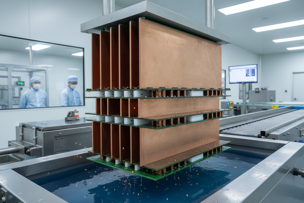
Manufacturing Process and Quality Control
Heavy Copper PCB Manufacturing Workflow
The manufacturing of heavy copper PCBs requires specialized equipment and processes:
1. Material Preparation and Inner Layer Processing
- High-Tg laminate selection with verified Tg and CTE specifications
- Thick copper foil lamination (3-20 oz starting copper)
- Precision etching with differential etch rates for thick copper
- Automated optical inspection (AOI) of inner layers
2. Drilling and Via Formation
- CNC drilling with optimized feeds/speeds for thick copper
- Controlled-depth drilling for blind and buried vias
- Plasma desmear for via cleaning and surface preparation
- Electroless copper deposition for via conductivity
3. Electroplating and Copper Build-Up
- Pulse-reverse plating for uniform via filling (85-95% fill ratio)
- Copper thickness verification with microsection analysis
- Surface preparation for outer layer imaging
- Megasonic-assisted deposition for high-aspect-ratio vias
4. Outer Layer Processing and Solder Mask
- Precision imaging with compensation for thick copper etching
- Differential etching control to maintain trace accuracy
- High-temperature solder mask (compatible with lead-free processes)
- Legend printing with industrial-grade inks
5. Surface Finish and Final Fabrication
- ENIG plating with 3-6µm nickel and 0.05-0.1µm gold
- Electrical testing (flying probe or bed-of-nails)
- Microsection analysis for copper thickness verification
- Final inspection per IPC-A-600 Class 3 standards
Quality Control and Testing Protocols
In-Process Inspection:
| Inspection Stage | Method | Defects Detected | Acceptance Criteria |
|---|---|---|---|
| Solder Paste Printing | SPI (3D) | Volume, height, offset | ±10% of target |
| Component Placement | AOI (2D/3D) | Missing, skewed, wrong part | IPC-A-610 Class 3 |
| Post-Reflow | AOI (3D) | Solder joints, bridging, tombstoning | IPC-A-610 Class 3 |
| BGA/QFN Inspection | X-Ray | Voids, bridging, head-in-pillow | <25% voids (Class 2), <15% (Class 3) |
| Electrical Test | ICT/Flying Probe | Opens, shorts, wrong values | 100% coverage |
| Functional Test | Custom Fixtures | Performance validation | Per specification |
Table 6: Quality control inspection matrix for heavy copper PCB assembly
Reliability Testing:
- Thermal cycling: -40°C to +125°C, 500-1000 cycles (IPC-TM-650 2.6.7)
- Thermal shock: 0°C to 100°C, 15-second transfer (IPC-TM-650 2.6.7.2)
- Vibration testing: 5-2000 Hz, 5-20g acceleration (MIL-STD-202 Method 204)
- Humidity exposure: 85°C/85% RH, 1000 hours (IPC-TM-650 2.6.14)
- Salt spray: 5% NaCl, 35°C, 96+ hours (ASTM B117)
Certifications and Standards Compliance
Essential Certifications for Industrial PCBs:
- IPC-A-610 Class 3: High-performance/high-reliability electronic assemblies
- IPC-6012 Class 3: Qualification and performance specification for rigid PCBs
- IPC-2152: Standard for determining current-carrying capacity
- ISO 9001:2015: Quality management systems
- IATF 16949:2016: Automotive quality management (relevant for industrial applications)
- UL 94: Flammability testing for safety-critical applications
- RoHS/REACH: Environmental compliance for lead-free manufacturing
Real-World Applications and Case Studies
Application 1: Motor Drive Control Systems
Challenge: A manufacturer of industrial motor drives needed PCBs to handle 150A continuous current with peak demands of 300A during motor startup. The boards operated in high-vibration environments near large motors, with ambient temperatures reaching 75°C.
Solution:
- 6 oz heavy copper PCB with High-Tg FR-4 substrate (Tg 170°C)
- Dedicated power and ground planes on internal layers
- Thermal via arrays beneath IGBT modules (4×4 grid, 0.3mm vias)
- ENIG surface finish for corrosion resistance
- Silicone conformal coating for vibration damping and moisture protection
Results:
- Zero field failures after 18 months of continuous operation
- Operating temperature reduced by 18°C compared to previous 4 oz design
- Vibration resistance improved by 75% (no solder joint failures)
- System efficiency improved by 3.2% due to reduced IR losses
Application 2: Solar Inverter Power Electronics
Challenge: A renewable energy company required PCBs for 50kW solar inverters operating in outdoor environments with temperature extremes of -40°C to +85°C. The boards needed to handle 1000V DC and 50A continuous with 20-year operational lifespan requirements.
Solution:
- 10 oz heavy copper PCB with polyimide substrate (Tg >260°C)
- Wide traces (0.030 inches) for high-voltage isolation
- Large copper pours for heat dissipation
- Immersion silver surface finish for excellent conductivity
- Urethane conformal coating for UV and moisture protection
Results:
- 80% reduction in heat-related downtime
- 20% increase in inverter efficiency due to superior thermal management
- Zero delamination after 1000 thermal cycles (-40°C to +85°C)
- Projected 25-year lifespan meeting customer requirements
Application 3: Battery Management System (BMS) for Industrial Vehicles
Challenge: An electric forklift manufacturer needed a compact BMS PCB to monitor and balance 48V battery packs with 200A continuous discharge. The system operated in warehouse environments with temperature cycling and moderate vibration.
Solution:
- 6 oz heavy copper PCB with High-Tg FR-4 and ENIG finish
- Integrated copper pours and thermal vias for heat dissipation
- Blind vias to save space in compact design
- Optimized trace width and spacing per IPC-2152 calculations
- Acrylic conformal coating for moisture and dust protection
Results:
- 15% reduction in BMS overall size compared to previous design
- 200A current handling without overheating (verified at 85°C ambient)
- IPC-A-610 Class 3 compliance achieved
- Zero field failures in first 10,000 units deployed
Application 4: PLC Controller for Chemical Processing
Challenge: A chemical plant needed PLC controller PCBs to operate in corrosive atmospheres with H₂S and SO₂ exposure, high humidity (up to 95% RH), and temperature cycling. System downtime costs exceeded $50,000 per hour.
Solution:
- 4 oz heavy copper PCB with High-Tg FR-4
- ENIG surface finish for superior corrosion resistance
- Epoxy conformal coating for chemical resistance
- Enhanced creepage and clearance distances for high-voltage isolation
- Vibration-resistant mounting and reinforced connectors
Results:
- 85% reduction in PCB-related downtime over 3-year period
- Zero corrosion-related failures after 2000-hour salt spray testing
- 10-year operational lifespan achieved without degradation
- ROI of 340% based on avoided downtime costs
Cost-Benefit Analysis and ROI
Understanding Heavy Copper PCB Costs
Heavy copper PCB manufacturing typically costs 2-5x more than standard PCBs, depending on copper weight, layer count, and complexity. However, total system cost often decreases due to eliminated components and improved reliability.
Cost Comparison (Prototype Quantities):
| PCB Type | 4-Layer, 100mm×150mm | Relative Cost | Lead Time |
|---|---|---|---|
| Standard 1 oz | $50–100 | 1.0x | 5–7 days |
| Thick 2 oz | $80–150 | 1.5x | 7–10 days |
| Heavy 4 oz | $200–400 | 3.0x | 10–15 days |
| Heavy 6 oz | $350–600 | 4.5x | 12–18 days |
| Extreme 10 oz | $600–1000 | 7.0x | 15–20 days |
Table 7: Relative cost comparison for heavy copper PCBs (prototype quantities)
Total Cost of Ownership Analysis
Direct Cost Savings:
- Eliminated External Components
- External heat sinks: $5-50 per board
- Bus bars and connectors: $10-30 per board
- Cooling fans: $3-15 per board
- Total savings: $18-95 per board
- Reduced Assembly Complexity
- Fewer assembly steps: 20-30% labor reduction
- Lower procurement costs: fewer BOM line items
- Reduced inventory management: fewer components to stock
- Improved Manufacturing Yield
- Heavy copper boards: 95-98% first-pass yield
- Standard boards with external cooling: 85-92% yield
- Reduced rework and scrap costs
Indirect Cost Savings:
- Extended Product Lifespan
- Standard industrial PCBs: 2-5 year lifespan
- Heavy copper PCBs: 10-15+ year lifespan
- 3x longer replacement cycle
- Reduced Field Failures
- 60-80% reduction in PCB-related failures
- Lower warranty costs and service calls
- Improved customer satisfaction and retention
- System Efficiency Gains
- 2-5% improvement in power conversion efficiency
- Reduced energy costs over product lifetime
- Lower cooling requirements
ROI Calculation Example
Scenario: Industrial motor drive system producing 10,000 units annually
Investment: Upgrading from 2 oz to 6 oz heavy copper PCBs
- Additional PCB cost: $250 per board
- Total additional investment: $2,500,000 (first year)
Annual Savings:
- Eliminated heat sinks and fans: $45 per board × 10,000 = $450,000
- Reduced assembly labor: $12 per board × 10,000 = $120,000
- Improved yield (3% gain): $30 per board × 300 = $9,000
- Reduced warranty claims (70% reduction): $200,000
- Energy efficiency gains (3% improvement): $150,000
- Total annual savings: $929,000
Payback Period: 2.7 years
5-Year ROI: 86% ($4,645,000 savings vs. $2,500,000 investment)
10-Year ROI: 272% ($9,290,000 savings vs. $2,500,000 investment)
When Heavy Copper Is Essential vs. Optional
Heavy Copper Is Essential When:
- Current requirements exceed 10A continuous
- Operating temperatures exceed 85°C ambient
- Thermal cycling exceeds 100 cycles during product lifetime
- Vibration environments exceed 5g acceleration
- System downtime costs exceed $5,000 per hour
- Product lifespan requirements exceed 5 years
- Safety-critical applications where failure is not an option
Standard Copper May Suffice When:
- Current requirements below 5A
- Controlled indoor environments (<50°C ambient)
- Low-vibration installations
- Short product lifespans (2-3 years)
- Cost-sensitive consumer applications
- Non-critical systems where downtime is acceptable
Frequently Asked Questions
What is the maximum current a heavy copper PCB can handle?
Current capacity depends on copper weight, trace width, and acceptable temperature rise. As a general guideline:
- 4 oz copper: 50-100A continuous per layer
- 6 oz copper: 100-200A continuous per layer
- 10 oz copper: 200-500A+ continuous per layer
For precise calculations, use IPC-2152 standards considering trace geometry, ambient temperature, and copper plane proximity. For currents above 100A, consider integrating copper bus bars into the PCB structure.
How does heavy copper PCB manufacturing differ from standard PCB fabrication?
Heavy copper manufacturing requires specialized processes:
- Extended plating times: 10-20+ hours vs. 1-2 hours for standard PCBs
- Differential etching: Step-etch techniques to maintain trace accuracy
- Pulse-reverse plating: For uniform via filling at high aspect ratios
- Controlled lamination: Higher pressure and precise temperature cycles
- Thicker starting materials: 3-20 oz copper foil vs. 0.5-2 oz standard
These specialized processes increase manufacturing time by 50-100% and cost by 200-500%, but deliver superior performance and reliability.
Can heavy copper and standard copper be combined on the same PCB?
Yes, modern manufacturing techniques allow “hybrid” or “PowerLink” constructions with different copper weights on different layers:
- Power layers: 4-6 oz copper for high-current paths
- Signal layers: 1-2 oz copper for control circuitry
- Optimized cost: Heavy copper only where needed
This approach reduces overall PCB cost by 20-40% compared to full heavy copper boards while maintaining performance where it matters most.
What surface finish is best for harsh environment industrial PCBs?
ENIG (Electroless Nickel Immersion Gold) is the recommended choice for harsh industrial environments:
- Superior corrosion resistance: Nickel barrier prevents copper oxidation
- Excellent solderability: Gold layer ensures reliable solder joints
- Long shelf life: 24+ months without degradation
- Flat surface: Ideal for fine-pitch components and BGA packages
- Wire bondable: Compatible with advanced assembly techniques
For extreme chemical environments, consider ENEPIG (Electroless Nickel Electroless Palladium Immersion Gold) for even better corrosion resistance, though at higher cost.
How do I specify heavy copper PCBs for my industrial application?
Key Specifications to Include:
- Copper weight per layer: Specify 3 oz, 4 oz, 6 oz, etc. for each layer
- Base material: High-Tg FR-4 (Tg ≥170°C) minimum for industrial apps
- Surface finish: ENIG for harsh environments
- Conformal coating: Type and thickness (e.g., silicone, 50µm)
- Quality standard: IPC-A-610 Class 3 for high-reliability
- Testing requirements: Thermal cycling, vibration, humidity
- Current capacity: Per IPC-2152 calculations with safety margin
- Environmental ratings: Operating temperature range, humidity, vibration
Work with your PCB manufacturer early in the design process to ensure specifications align with their capabilities and to optimize cost-performance trade-offs.
What is the typical lead time for heavy copper PCB prototypes?
Standard Lead Times:
- 3-4 oz copper: 10-15 working days
- 6 oz copper: 12-18 working days
- 10+ oz copper: 15-25 working days
Expedited Options:
Many manufacturers offer quick-turn services for heavy copper prototypes:
- 5-day expedite: Typically 50-100% cost premium
- 3-day super-expedite: 100-200% cost premium
Lead times are longer than standard PCBs due to extended plating cycles and specialized processing requirements.
How does conformal coating impact PCB thermal performance?
Conformal coating has minimal impact on thermal performance when properly applied:
- Thermal conductivity: 0.2-0.3 W/mK (similar to FR-4)
- Thickness: 25-75µm (thin relative to PCB thickness)
- Impact: <5% increase in thermal resistance
However, coating over heat-generating components (like heat sinks or thermal pads) can reduce heat dissipation. Always mask thermal interfaces before conformal coating application.
Can heavy copper PCBs be repaired or reworked?
Heavy copper PCBs are more challenging to rework than standard boards due to increased thermal mass:
- Soldering: Requires higher temperatures and longer dwell times
- Component removal: More difficult due to heat sinking effect of thick copper
- Trace repair: Possible with specialized equipment and skilled technicians
- Success rate: 70-85% vs. 90-95% for standard PCBs
Best practice: Design for manufacturability (DFM) to minimize rework needs, and work with experienced technicians for any required repairs.
Conclusion and Next Steps
Key Takeaways
Industrial control systems operating in harsh environments demand PCB solutions that go far beyond standard consumer-grade specifications. Heavy copper PCB assembly provides the current-carrying capacity, thermal management, and mechanical durability essential for reliable long-term operation.
Critical Success Factors:
- Material Selection: High-Tg FR-4 (Tg ≥170°C) or polyimide substrates for temperature resilience
- Copper Weight: 4-6 oz minimum for high-current applications (50A+)
- Thermal Management: Integrated thermal vias, copper pours, and strategic component placement
- Environmental Protection: ENIG surface finish + conformal coating for corrosion resistance
- Quality Standards: IPC-A-610 Class 3 + comprehensive reliability testing
- Design Optimization: IPC-2152 compliance for trace sizing and current capacity
The Business Case for Heavy Copper Solutions
While heavy copper PCBs cost 2-5x more than standard boards, the total cost of ownership often favors heavy copper when considering:
- Eliminated external components (heat sinks, bus bars, cooling fans)
- Reduced assembly complexity and improved yields
- Extended product lifespan (10-15+ years vs. 2-5 years)
- 60-80% reduction in field failures and warranty costs
- 2-5% improvement in system efficiency
- Typical ROI: 80-300% over 5-10 years
Your Next Steps
For New Designs:
- Assess your requirements: Current capacity, temperature range, vibration, environmental exposure
- Calculate total cost of ownership: Include avoided downtime and extended lifespan
- Engage a qualified manufacturer early: Ensure DFM alignment and capability verification
- Prototype and validate: Thermal testing, vibration testing, environmental exposure
- Plan for scale: Confirm production capacity and supply chain stability
For Existing Products:
- Analyze field failure data: Identify PCB-related issues and root causes
- Calculate cost of failures: Downtime, warranty, service calls, reputation damage
- Evaluate upgrade feasibility: Retrofit vs. redesign vs. next-generation product
- Pilot heavy copper solution: Limited deployment with comprehensive monitoring
- Measure results: Failure rates, operating temperatures, customer satisfaction
Partner with Experts in Heavy Copper PCB Assembly
Successfully implementing heavy copper solutions requires expertise in design, manufacturing, and quality control. Look for partners with:
- Proven heavy copper capability: 4-20 oz copper with documented quality
- Industrial application experience: Case studies in your specific industry
- Comprehensive quality systems: IPC Class 3, ISO 9001, IATF 16949
- Advanced testing capabilities: Thermal cycling, vibration, environmental simulation
- Design support: DFM review, thermal analysis, IPC-2152 calculations
- Supply chain stability: Material sourcing, component procurement, production scaling
PCB assembly services from experienced manufacturers like Andwin Circuits provide the expertise, capabilities, and quality systems necessary to deliver heavy copper solutions that perform reliably in the world’s harshest industrial environments.