
Lifting the “veil” of electromagnetic compatibility of PCB board 2
The changing electric field produces the changing magnetic field, and the changing magnetic field produces the changing electric field. This is the principle of electromagnetic wave generation and transmission. The changing magnetic field is generated by the change of magnetic flux in the line through which the changing current flows, because this introduces electromagnetic interference, which is the most troublesome thing for our electronic engineers. So from the root, controlling the magnetic flux of the circuit board is an important means to prevent electromagnetic interference of the circuit board.
When we draw the board, we often hear a sentence that is to make the loop as small as possible. Now let’s take a look at a simple explanation.
As shown in the left side of the above figure, the PCB routing diagram Figure, using electromagnetic field knowledge, we can know (if the signal frequency of the routing loop is high enough), then this board becomes a good antenna, and the circuit board design becomes a mess. The electromagnetic interference generated by the routing on the right is much smaller, which is the idea of minimizing the magnetic flux of the circuit board (that is, what we often call loop minimization).
Using a mirror plane when designing is a good choice, which can effectively eliminate the impact of interference generated by the power supply or ground plane on the electronic circuit.
The mirror plane refers to the plane that constitutes the return flow, such as the power supply and ground plane at most levels, but there are also power supplies and power planes that are mirror planes, such as RS232 level, etc. The mirror plane can also be regarded as a differential signal. The differential signal has a good inhibitory effect on common mode interference. The distance between the mirror planes should be as small as possible. If it is a double-sided board or a single-sided board, it is a good method to copper-plated on both sides and make more vias. Generally, do not stack two unrelated power planes together, especially when the voltage difference is large, otherwise the mutual interference of power supplies will become serious due to the effect of capacitive coupling. No matter how well the PCB wiring is designed, the magnetic field and electric field will always exist, but if the magnetic flux is reduced or eliminated, the EMI will become very small or non-existent.
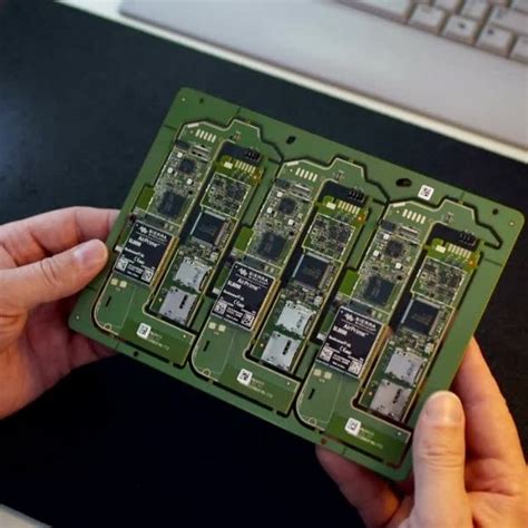
When designing PCB When designing a board, you can reduce the signal line loop of the board (reduce the magnetic flux generated by the signal line) through good routing to reduce interference. I have summarized the following methods:
- When designing a multi-layer board, you should follow the multi-layer board stacking settings and signal line impedance control. For the top layer, power supply, ground and bottom layers of a 4-layer board, this can greatly solve the electromagnetic interference problem and improve the reliability of the system. On the other hand, it can improve the wiring rate of the wire and reduce the area of the PCB board. A 6-layer board usually adds 2 signal layers on the basis of a 4-layer board. An 8-layer board usually includes 1 power layer, two ground layers, and 5 signal layers. For layer settings, there is a wealth of information on the Internet, or you can leave a message to discuss. For impedance control of routing, we often use SI9000 for design;
- Keep the clock routing as short and close to the ground as possible. For multi-layer boards, do not route key signal lines. Single-sided and double-sided boards can use ground routing Wire or protection wiring;
- For RF chips or high-frequency chips, the Faraday cage method can be used to shield and ground them, leaving only the input and output and power supply connections to the outside;
- Select appropriate component modules, concentrate the operating frequency in a narrower frequency band, and reduce electromagnetic interference through hardware processing;
- For RF circuits, use a lower driving voltage to reduce the RF current of the wiring, thereby achieving the effect of reducing the magnetic flux of the signal loop;
- Reduce the ground noise voltage, which can provide an enhanced path for the return current and map the image current back to the current source;
- For large capacitive loads, pay attention to the use of decoupling circuits;
- Appropriately introduce data line filters and common mode chokes, which can greatly improve the electromagnetic characteristics of the board;
- Pay attention to the use of bypass capacitors and decoupling capacitors, but this does not mean that the more the better.
Of course, the above methods can be used to solve the electromagnetic interference inside the PCB, but there are other reasons that can also cause electromagnetic interference, such as: there are common-mode and differential-mode currents between the circuit and the I/O connection, the ground loop will produce a magnetic field structure, the components will radiate and the impedance is not matched, etc. If the designed PCB board has electromagnetic interference, find the interference source through the idea of module measurement, and adopt targeted solutions to achieve the purpose of eliminating electromagnetic interference.
The above are some methods I have summarized to reduce the electromagnetic interference of PCB circuits. If there are any unreasonable places, please leave a message to criticize and correct. Welcome everyone to leave a message and discuss the problems of electronic design together, and make our design more mature through communication.