Low-Power Technologies for IC, Packaging, and PCB Design: A Comprehensive Review
Abstract
This paper explores the latest advancements in low-power design techniques across integrated circuits (IC), packaging technologies, and printed circuit boards (PCB). As electronic devices become increasingly pervasive in our daily lives while facing growing demands for energy efficiency, the development of low-power solutions has become critical for sustainable technological progress. We examine power optimization strategies at each level of electronic system design, from transistor-level innovations to system-level architectural approaches, and discuss how these techniques interact across different hierarchy levels to achieve maximum energy efficiency.
Keywords: low-power design, power management, IC design, advanced packaging, PCB optimization, energy efficiency
1. Introduction
The relentless growth of electronic devices in all aspects of modern life—from mobile gadgets to massive data centers—has made power consumption a primary concern for designers. With global electricity demand for information and communication technology estimated to reach 8% of worldwide usage by 2030, low-power design has evolved from a competitive advantage to an environmental and economic necessity.
This paper presents a holistic view of low-power technologies spanning three critical domains:
- Integrated Circuit (IC) level techniques
- Advanced packaging solutions
- PCB design methodologies
We analyze how innovations at each level contribute to overall system power reduction and how these domains interact to create synergistic effects in power optimization.

2. Low-Power IC Design Techniques
2.1 Transistor-Level Optimization
Modern ICs employ numerous transistor-level techniques to minimize power consumption:
FinFET and Nanosheet Transistors: These 3D transistor structures provide better channel control than planar MOSFETs, enabling lower leakage currents and reduced operating voltages. Intel’s RibbonFET (gate-all-around) technology demonstrates 30-50% lower power at constant performance compared to FinFET.
Multi-Threshold Voltage Design: By using high-Vt transistors in non-critical paths and low-Vt transistors where performance is crucial, designers can optimize the speed-power tradeoff. TSMC’s N5P process offers five different threshold voltages for such optimization.
Subthreshold Operation: For ultra-low-power applications like IoT sensors, circuits operate in the subthreshold region where currents are exponentially smaller. ARM’s Cortex-M0+ implemented in subthreshold CMOS achieves active power below 10μW/MHz.
2.2 Circuit-Level Techniques
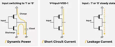
Power Gating: This technique completely shuts off power to inactive circuit blocks using header/footer switches. Intel’s 22nm FFL (Fine-Grained Power Gating) technology reduces leakage by 5-10× in idle modes.
Dynamic Voltage and Frequency Scaling (DVFS): Modern processors like Apple’s M-series chips dynamically adjust voltage and frequency based on workload, achieving up to 60% power savings for light workloads.
Near-Threshold Computing (NTC): Operating slightly above the threshold voltage balances performance and power. The University of Michigan’s Phoenix processor demonstrated 10× energy efficiency improvement using NTC.
2.3 Architectural Approaches
Heterogeneous Computing: Combining high-performance cores with efficiency cores (as in ARM’s big.LITTLE architecture) allows workloads to run on the most power-appropriate processing elements.
Approximate Computing: For error-tolerant applications like multimedia, intentionally allowing small computational errors can yield significant power savings. NVIDIA’s DLSS technology uses this principle in graphics processing.
Clock Domain Optimization: Dividing designs into multiple clock domains with localized clock gating reduces dynamic power. AMD’s Zen architecture uses over 1000 individual clock domains.
3. Low-Power Packaging Technologies
3.1 Advanced Packaging Architectures
2.5D and 3D Integration: Technologies like TSMC’s CoWoS (Chip on Wafer on Substrate) and Intel’s Foveros allow shorter interconnects between dies, reducing communication energy. 3D stacking can lower interconnect power by 10-100× compared to traditional packaging.
Chiplet-Based Design: Breaking large SoCs into smaller chiplets (as in AMD’s EPYC processors) enables better power management of individual functional blocks and reduces unnecessary switching activity across the entire die.
3.2 Power Delivery Network (PDN) Optimization
Integrated Voltage Regulators: Moving voltage regulation onto the package (like Intel’s Fully Integrated Voltage Regulator) reduces I²R losses in power delivery. This approach shows 20-30% improved power efficiency.
3D Power Delivery Networks: Using through-silicon vias (TSVs) and micro-bumps for vertical power delivery minimizes resistive losses. IMEC’s 3D PDN technology demonstrates 40% lower IR drop compared to planar approaches.
3.3 Thermal Management
Embedded Microfluidic Cooling: DARPA’s ICECool program demonstrated packages with integrated microchannels that enable direct liquid cooling, reducing the energy needed for thermal management by 50%.
Phase Change Materials (PCMs): Integrating materials like paraffin wax into packages provides passive thermal buffering, smoothing peak temperature spikes that would otherwise require higher cooling energy.
4. Low-Power PCB Design Methodologies
4.1 Power Integrity Optimization
Decoupling Capacitor Placement: Strategic placement of decoupling capacitors (like Intel’s FIVR-compatible PCB designs) reduces power rail noise, allowing lower operating voltages.
Power Plane Optimization: Techniques like buried capacitance (from companies like ZBC) and optimized plane shapes minimize AC impedance, reducing power loss in distribution.
4.2 Signal Integrity for Power Efficiency
Impedance Matching: Proper termination (as specified in USB4 and PCIe 5.0 standards) prevents signal reflections that cause unnecessary retransmissions and power waste.
Low-Loss Materials: High-frequency laminates like Rogers’ RO4000® series reduce dielectric losses, enabling lower transmit power for the same signal integrity.
4.3 Board-Level Power Management
Distributed Power Architecture: Instead of centralized conversion, point-of-load regulators (like Vicor’s Factorized Power) minimize I²R losses in power distribution.
Energy Harvesting Integration: Modern PCBs increasingly incorporate energy harvesting circuits (from companies like e-peas) for auxiliary power needs, reducing main power rail loading.
5. Cross-Domain Power Optimization
The most significant power savings emerge when considering interactions between IC, package, and PCB:
Co-Design of PDNs: Collaborative design of on-chip, package, and board-level power delivery (as in NVIDIA’s GPU designs) can reduce total power loss by 25-40%.
Thermal-Aware Floorplanning: Considering heat generation at IC level, dissipation through package, and PCB cooling capacity enables optimal performance per watt.
Signal/Power Co-Optimization: Simultaneous design of signal and power integrity across all levels (pioneered by IBM’s SiGe designs) minimizes unnecessary overhead.
6. Emerging Technologies and Future Directions
Optical Interconnects: Replacing electrical connections with optical links (like Ayar Labs’ optical I/O) could reduce communication energy by an order of magnitude.
Cryogenic CMOS: Operating chips at cryogenic temperatures (as explored by Google for quantum computing) dramatically reduces power, though currently with significant cooling overhead.
Neuromorphic Architectures: Brain-inspired designs like Intel’s Loihi 2 demonstrate 1000× better energy efficiency for certain workloads through massive parallelism and event-driven operation.
7. Conclusion
The pursuit of lower power consumption in electronic systems requires innovations at all levels of the design hierarchy—from nanometer-scale transistors to centimeter-scale PCBs. As this paper demonstrates, the most significant improvements come not from isolated optimizations, but from co-design approaches that consider the entire system. Future advancements will likely focus on tighter integration across domains, novel materials, and more intelligent power management systems that dynamically adapt to operational needs.
The semiconductor industry’s continued progress in low-power technologies will be crucial for enabling next-generation applications—from ubiquitous IoT to advanced AI—while addressing global energy challenges. As process scaling becomes increasingly difficult, architectural and system-level innovations will play an ever-greater role in achieving the energy efficiency needed for sustainable computing growth.