
Methods and analysis of anti-ESD in PCB design
Static electricity from the human body, environment, and even inside electronic devices can cause various damages to precision semiconductor chips, such as penetrating the thin insulation layer inside the components; damaging the gate of MOSFET and CMOS components; locking the trigger in the CMOS device; short-circuiting the reverse-biased PN junction; short-circuiting the forward-biased PN junction; melting the welding wire or aluminum wire inside the active device. In order to eliminate the interference and damage of electrostatic discharge (ESD) to electronic equipment, a variety of technical means need to be taken to prevent it.
In the design of PCB boards, the anti-ESD design of PCBs can be achieved through layering, proper layout and installation. In the design process, most design modifications can be limited to adding or removing components through prediction. By adjusting the PCB layout and wiring, ESD can be well prevented.

The following are some common preventive measures.
- Use multi-layer PCBs as much as possible. Compared with double-sided PCBs, ground planes and power planes, as well as closely arranged signal line-ground line spacing can reduce common-mode impedance and inductive coupling to 1/10 to 1/100 of double-sided PCBs. Try to keep each signal layer close to a power or ground layer. For high-density PCBs with components on both the top and bottom surfaces, very short connection lines, and many fills, consider using inner layer lines.
- For double-sided PCBs, use tightly interwoven power and ground grids. Power lines are close to ground lines, and as many connections as possible between vertical and horizontal lines or fill areas. The grid size on one side is less than or equal to 60mm, and if possible, the grid size should be less than 13mm.
- Make each circuit as compact as possible.
- Place all connectors on one side as much as possible.
- If possible, bring power lines in from the center of the card and away from areas that are easily directly affected by ESD.
- Place wide chassis ground or polygonal fill on all PCB layers below connectors that lead out of the chassis (which are easily directly hit by ESD), and connect them together with vias every approximately 13mm.
- Place mounting holes on the edge of the card, and connect the mounting holes to the chassis ground with top and bottom pads without solder mask around them.
- Do not apply any solder to the top or bottom pads when assembling the PCB. Use screws with built-in washers to achieve close contact between the PCB and the metal chassis/shield or bracket on the ground plane.
- Set the same “isolation zone” between the chassis ground and circuit ground on each layer; if possible, keep the spacing distance at 0.64mm.
- Connect the chassis ground and circuit ground together with a 1.27mm wide wire along the chassis ground line every 100mm near the mounting holes on the top and bottom layers of the card. Place mounting pads or mounting holes between the chassis ground and circuit ground adjacent to these connection points. These ground connections can be cut with a blade to keep them open, or jumpered with ferrite beads/high-frequency capacitors.
- If the circuit board will not be placed in a metal chassis or shield, do not apply solder mask to the top and bottom chassis grounds of the circuit board so that they can act as discharge electrodes for ESD arcs.
- Set up a ring ground around the circuit in the following manner:
(1) Place a ring ground path around the entire periphery, except for the edge connector and chassis ground.
(2) Make sure the width of the ring ground on all layers is greater than 2.5mm.
(3) Connect the ring ground with vias every 13mm.
(4) Connect the ring ground to the common ground of the multi-layer circuit.
(5) For double-sided boards installed in a metal chassis or shield, the ring ground should be connected to the circuit common ground. Unshielded double-sided circuits should connect the ring ground to the chassis ground. Do not apply solder mask to the ring ground so that the ring ground can act as a discharge rod for ESD. Place at least a 0.5mm wide gap somewhere on the ring ground (all layers) to avoid forming a large loop. The distance between the signal wiring and the ring ground cannot be less than 0.5mm.
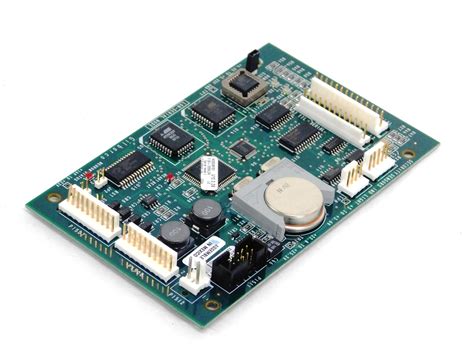
- In areas that can be directly hit by ESD, a ground wire must be laid near each signal line.
- The I/O circuit should be as close to the corresponding connector as possible.
- Circuits that are susceptible to ESD should be placed in an area close to the center of the circuit so that other circuits can provide them with a certain shielding effect.
- Resistors and magnetic beads are usually placed in series at the receiving end, and for cable drivers that are susceptible to ESD, you can also consider placing resistors or magnetic beads in series at the driving end.
- Transient protectors are usually placed at the receiving end. Use short and thick wires (less than 5 times the width, preferably less than 3 times the width) to connect to the chassis ground. The signal line and ground wire coming out of the connector should be directly connected to the transient protector before connecting to other parts of the circuit.
- Filter capacitors should be placed at the connector or within 25mm of the receiving circuit.
(1) Use short and thick wires to connect to the chassis ground or receiving circuit ground (less than 5 times the width, preferably less than 3 times the width).
(2) The signal line and ground line are first connected to the capacitor and then to the receiving circuit.
- Make sure the signal line is as short as possible.
- When the length of the signal line is greater than 300mm, a ground line must be laid in parallel.
- Make sure the loop area between the signal line and the corresponding loop is as small as possible. For long signal lines, the positions of the signal line and the ground line should be swapped every few centimeters to reduce the loop area.
- Drive the signal into multiple receiving circuits from the center of the network.
- Make sure the loop area between the power supply and the ground is as small as possible, and place a high-frequency capacitor close to each power pin of the integrated circuit chip.
- Place a high-frequency bypass capacitor within 80mm of each connector.
- Where possible, fill unused areas with ground, and connect the filled ground of all layers every 60mm.
- Make sure that the two opposite end positions of any large ground fill area (approximately greater than 25mm×6mm) are connected to the ground.
- When the length of the opening on the power or ground plane exceeds 8mm, use a narrow line to connect the two sides of the opening.
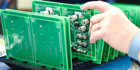
*Reset lines, interrupt signal lines, or edge-triggered signal lines should not be placed near the edge of the PCB.
*Connect the mounting holes to the circuit common ground or isolate them.
(1) When a metal bracket must be used with a metal shield or chassis, a zero-ohm resistor should be used to achieve the connection.
(2) Determine the size of the mounting hole to achieve reliable installation of the metal or plastic bracket. Use large pads on the top and bottom layers of the mounting hole. Do not use solder resist on the bottom pad, and ensure that the bottom pad is not soldered using a wave soldering process.
*Protected signal lines and unprotected signal lines cannot be arranged in parallel.
*Pay special attention to the routing of reset, interrupt, and control signal lines.
(1) Use high-frequency filtering.
(2) Keep away from input and output circuits.
(3) Keep away from the edge of the circuit board.
*The PCB should be inserted into the chassis and should not be installed in an opening or internal seam.
*Pay attention to the routing of signal lines under the ferrite beads, between pads, and where they may come into contact with the ferrite beads. Some magnetic beads are very conductive and may create unexpected conductive paths.
*If a chassis or motherboard is to contain several circuit boards, the most static-sensitive circuit board should be placed in the middle.