Microsection Analysis of PCB: Techniques and Applications
Introduction
Printed Circuit Boards (PCBs) are the backbone of modern electronics, providing the necessary interconnections between components. As PCBs become more complex with higher layer counts, finer traces, and advanced materials, ensuring their quality and reliability is critical. One of the most effective methods for inspecting PCB quality is microsectioning (also known as cross-sectioning or metallographic preparation). This technique involves cutting, polishing, and examining a small section of the PCB under a microscope to evaluate its internal structure.
This article explores the process of microsection analysis, its importance in PCB manufacturing and failure analysis, and the key observations that can be made using this technique.
1. What is PCB Microsectioning?
Microsectioning is a destructive testing method where a small sample of the PCB is cut, embedded in resin, polished, and examined under high magnification. This allows engineers to inspect:
- Layer alignment (registration between layers)
- Copper thickness and uniformity
- Plating quality (electroless and electrolytic copper)
- Solder mask adhesion and thickness
- Via and through-hole integrity (barrel cracks, voids, plating thickness)
- Delamination or resin recession
- Intermetallic compound (IMC) formation in solder joints
The process provides cross-sectional views of critical areas, helping identify manufacturing defects, material inconsistencies, and potential failure points.
2. Steps in PCB Microsection Preparation
2.1 Sample Selection and Cutting
- Identify the area of interest (e.g., a via, solder joint, or trace).
- Use a precision saw or laser cutter to extract a small sample (~1 cm²).
- Avoid excessive heat or mechanical stress that could alter the sample.
2.2 Encapsulation (Potting)
- The sample is embedded in epoxy resin to maintain structural integrity during polishing.
- Vacuum impregnation may be used to eliminate air bubbles.
2.3 Grinding and Polishing
- Coarse grinding removes excess material (~400-600 grit SiC paper).
- Fine grinding (~800-1200 grit) prepares the surface for polishing.
- Diamond or alumina polishing (1 µm to 0.05 µm) ensures a mirror-like finish.
2.4 Etching (Optional)
- Chemical etching (e.g., ferric chloride for copper) enhances contrast between layers.
- Helps distinguish grain boundaries and plating layers.
2.5 Microscopic Examination
- Optical microscopy (50x–1000x) provides initial inspection.
- Scanning Electron Microscopy (SEM) offers higher resolution and elemental analysis (EDS).
3. Key Observations in PCB Microsection Analysis
3.1 Plating Thickness and Uniformity
- Electroplated copper in vias should meet IPC standards (typically ≥ 25 µm for Class 2, ≥ 20 µm for Class 3).
- Uneven plating can lead to weak spots and eventual failure.
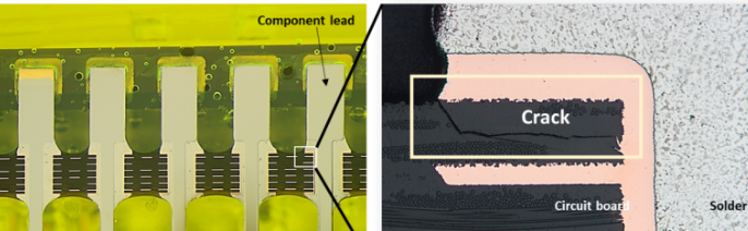
3.2 Via and Through-Hole Integrity
- Barrel cracks (from thermal stress or poor drilling).
- Voids or nodules (due to improper plating).
- Resin smear (leftover material from drilling, affecting connectivity).
3.3 Solder Joint Quality
- Intermetallic compounds (IMCs) should be uniform (Cu₆Sn₅, Cu₃Sn in copper-based solders).
- Kirkendall voids (excessive voids weaken joints).
- Solder wetting (poor wetting indicates contamination or oxidation).
3.4 Layer-to-Layer Alignment
- Misregistration between layers can cause short circuits or open connections.
- Dielectric thickness must be consistent to prevent impedance variations.
3.5 Delamination and Resin Recession
- Thermal stress can cause separation between layers.
- Moisture absorption leads to “popcorning” in reflow soldering.
4. Applications of PCB Microsectioning
4.1 Quality Control in Manufacturing
- Ensures compliance with IPC-A-600, IPC-6012 standards.
- Detects plating defects, voids, and layer misalignment before assembly.
4.2 Failure Analysis
- Identifies root causes of open circuits, short circuits, or intermittent failures.
- Helps in reverse engineering competitor PCBs (for benchmarking).
4.3 Reliability Testing
- Evaluates thermal cycling, mechanical stress, and corrosion resistance.
- Assesses high-frequency signal integrity by examining dielectric layers.
4.4 Research and Development
- Tests new materials (high-Tg, low-loss dielectrics).
- Validates advanced via technologies (laser microvias, stacked vias).
5. Challenges and Best Practices
5.1 Common Pitfalls
- Over-polishing can smear soft metals (e.g., solder).
- Contamination from improper cleaning affects imaging.
- Sample preparation artifacts (e.g., scratches, chipping).
5.2 Best Practices
- Use automated polishing systems for consistency.
- Document each step (cutting angle, polishing time, etching duration).
- Compare with reference standards (IPC guidelines).
6. Conclusion
Microsection analysis is an essential tool for PCB inspection, offering unparalleled insights into internal structures. Whether for quality assurance, failure analysis, or R&D, this technique helps ensure reliability and performance in modern electronics. By following standardized preparation methods and leveraging advanced microscopy, engineers can detect defects early, improve manufacturing processes, and enhance product longevity.
As PCB technology advances with HDI (High-Density Interconnect), flexible circuits, and embedded components, microsectioning will remain a critical inspection method for ensuring robust and reliable electronic assemblies.