
Multilayer PCB Stackup: 4 Layer vs 6 Layer vs 8 Layer Comparison
Choosing the right layer count isn’t about fitting traces—it’s about balancing signal integrity, EMI performance, power distribution, and cost. After designing over 200 multilayer boards at Andwin Circuits, I’ve learned that a poorly chosen stackup turns promising designs into costly redesign cycles.
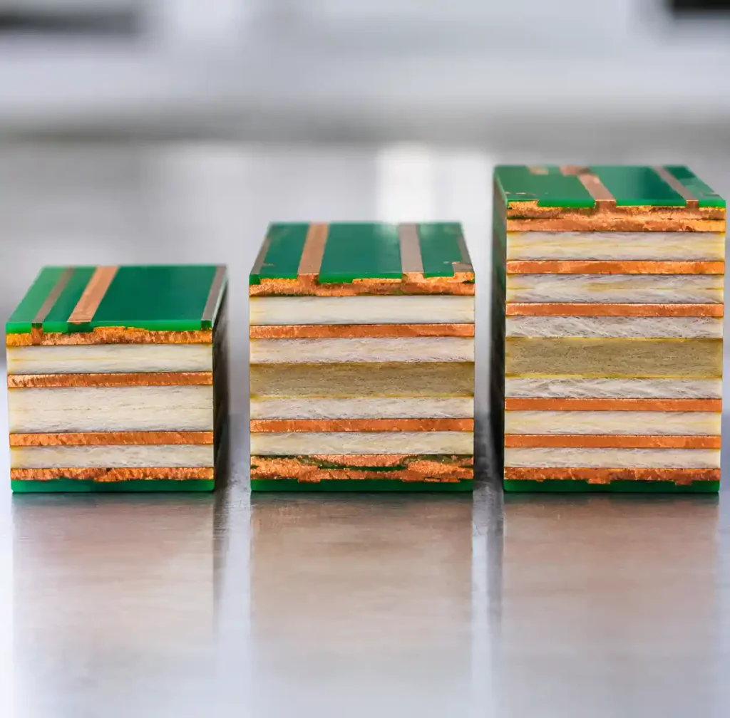
This guide breaks down when to use 4-layer, 6-layer, or 8-layer stackups based on real constraints: signal speed, power requirements, impedance control needs, and budget.
Understanding PCB Layer Stackup Fundamentals
A PCB stackup defines the arrangement of copper layers, prepreg, and core materials. Each layer serves a specific function: signal routing, ground planes, or power distribution. The stackup directly impacts characteristic impedance, signal return paths, and EMC performance.
Modern designs rarely succeed with just routing space calculations. A 4-layer board might offer enough area to route all traces, but without proper ground plane separation, you’ll face impedance discontinuities and failed EMI testing.
The choice between 4, 6, or 8 layers hinges on signal frequency (above 50MHz demands tighter impedance control), power delivery network complexity (multiple voltage rails favor dedicated power planes), and EMI requirements (stricter emission limits push toward more layers).
4-Layer PCB Stackup: When It’s Enough
A 4-layer board uses the classic Sig-GND-PWR-Sig configuration. Two inner layers serve as continuous reference planes—one ground, one power—with signal traces on outer layers. This arrangement works when your design operates below 100MHz, requires only 2-3 voltage rails, and doesn’t face stringent EMI limits.
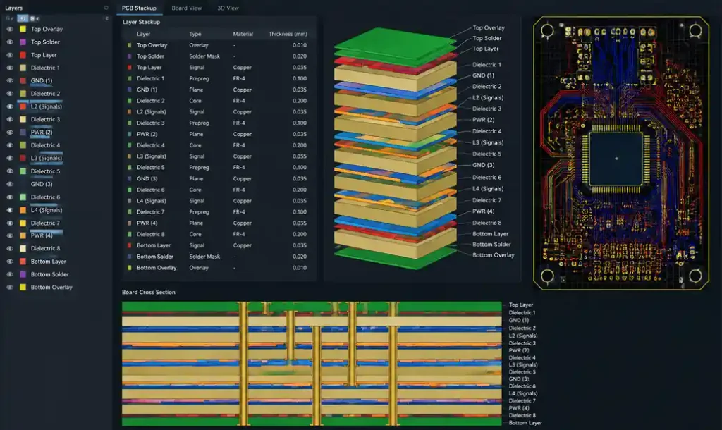
Typical 4-Layer Configuration
| Layer | Function | Thickness | Material |
|---|---|---|---|
| L1 (Top) | Signal | 1 oz (35µm) copper | – |
| L2 | Ground Plane | 1 oz copper | 0.2mm prepreg |
| L3 | Power Plane | 1 oz copper | 1.0mm core |
| L4 (Bottom) | Signal | 1 oz (35µm) copper | 0.2mm prepreg |
This stackup provides 50Ω or 90Ω differential impedance control with ±10% tolerance. The 0.2mm prepreg spacing between signal and ground layers delivers adequate return path coupling for signals up to 100MHz.
When 4 Layers Work
Use 4-layer stackups for microcontroller-based designs with clock speeds under 100MHz, simple IoT devices with 3.3V and 5V rails, industrial controls without high-speed serial interfaces, and consumer electronics where cost dominates. A typical 100x100mm 4-layer board costs $2-3 per unit at 1000-piece volumes.
The limitation appears when you add high-speed interfaces. USB 2.0 (480Mbps) barely fits 4-layer impedance control. USB 3.0, PCIe, HDMI, or Gigabit Ethernet all demand better stackup symmetry and tighter impedance tolerance than 4 layers deliver reliably.
6-Layer PCB Stackup: The High-Speed Sweet Spot
Six-layer boards add routing flexibility and EMI control without the cost jump of 8 layers. The optimal configuration places signal layers adjacent to ground planes, creating two controlled impedance routing environments with dual ground planes for superior return path management.
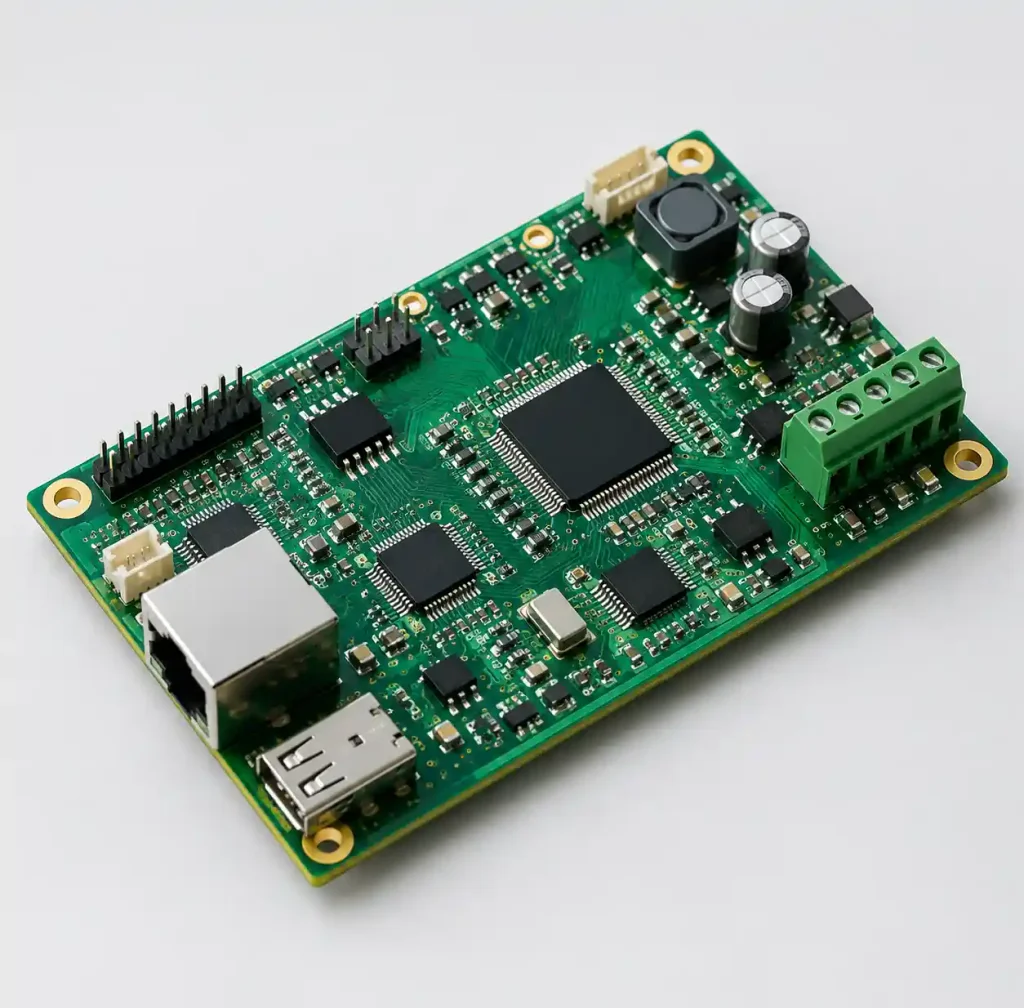
Recommended 6-Layer Configuration
| Layer | Function | Thickness | Impedance Zone |
|---|---|---|---|
| L1 | High-speed signals | 0.5 oz copper | Stripline (inner) |
| L2 | Ground plane | 1 oz copper | – |
| L3 | Signal routing | 1 oz copper | Stripline |
| L4 | Signal routing | 1 oz copper | Stripline |
| L5 | Ground plane | 1 oz copper | – |
| L6 | Power + low-speed | 0.5 oz copper | – |
This stackup delivers ±5% impedance tolerance and supports signals up to 5GHz. The dual ground planes provide two continuous reference paths, eliminating ground bounce issues common in 4-layer designs.
6-Layer Performance Advantages
The second ground plane cuts radiated emissions by 15-20dB compared to 4-layer boards at frequencies above 200MHz. This margin often means the difference between passing or failing FCC Class B or CE EMC testing on the first attempt.
Controlled impedance improves dramatically. Where 4-layer boards struggle to hold ±10% tolerance, 6-layer stackups achieve ±5% across the entire signal path. This matters for DDR3/DDR4 memory interfaces where timing margins demand tight impedance matching.
The cost increase over 4-layer boards runs 40-60%. A 100x100mm 6-layer board costs $3.50-5.00 per unit at 1000 pieces. For designs targeting high-speed data rates or strict EMI requirements, this cost pays for itself by eliminating expensive board spins.
8-Layer PCB Stackup: High-Performance Design
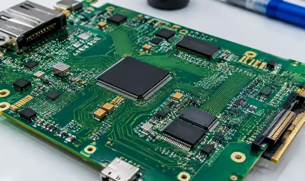
Eight-layer boards dominate high-speed digital designs: multi-gigabit serial links, DDR4 memory systems, RF subsystems, and applications where signal integrity cannot be compromised. Additional layers enable symmetric stripline routing, multiple power planes for clean PDN design, and dedicated ground planes for sensitive analog sections.
Standard 8-Layer Configuration
| Layer | Function | Copper Weight | Signal Type |
|---|---|---|---|
| L1 | High-speed signals | 0.5 oz | USB 3.0, PCIe, HDMI |
| L2 | Ground plane | 1 oz | Primary reference |
| L3 | High-speed routing | 1 oz | DDR4, high-speed serial |
| L4 | Power plane (+3.3V, +1.8V) | 1 oz | Split or solid |
| L5 | Power plane (+5V, +12V) | 1 oz | Split or solid |
| L6 | Signal routing | 1 oz | Medium-speed signals |
| L7 | Ground plane | 1 oz | Secondary reference |
| L8 | Power + low-speed | 0.5 oz | Connectors, debug |
This configuration creates two symmetric stripline environments with identical impedance characteristics. Symmetric stripline reduces crosstalk by 10-15dB compared to asymmetric 6-layer designs.
When 8 Layers Become Necessary
Move to 8 layers when your design includes DDR4 memory running at 2400MT/s or faster, multi-lane PCIe Gen 3/4, 10 Gigabit Ethernet, HDMI 2.0 or DisplayPort, RF sections requiring >50dB isolation, or six or more voltage rails with tight ripple specifications.
The cost penalty over 6 layers runs 50-70%. A 100x100mm 8-layer board costs $6-8.50 per unit at 1000 pieces. However, first-pass success rate for complex designs jumps significantly. Where 6-layer high-speed designs often need 2-3 spins, properly designed 8-layer boards typically pass on the first build.
Layer Count Selection Criteria
The decision tree starts with signal frequency. Below 50MHz, 4 layers suffice with only 2-3 power rails. From 50-500MHz, 6 layers provide adequate performance unless you’re running parallel buses like DDR memory. Above 500MHz or with multi-gigabit serial links, 8 layers become the baseline.
Power distribution network requirements push layer count independent of signal speed. Designs with 5+ voltage rails struggle on 4-layer stackups because power plane splitting creates ground discontinuities. Each voltage rail ideally occupies its own plane area.
EMI requirements increasingly drive layer selection. FCC Class B limits are achievable with 6 layers if you follow good layout practices. Medical (IEC 60601-1-2) and automotive (CISPR 25) standards frequently demand 8 layers to meet radiated emission limits.
| Design Parameter | 4-Layer | 6-Layer | 8-Layer |
|---|---|---|---|
| Max Signal Frequency | <100MHz | 500MHz-2GHz | >2GHz |
| Impedance Tolerance | ±10% | ±5% | ±3% |
| Power Rails | 2-3 | 3-5 | 5+ |
| Cost Multiplier | 1.0x | 1.5-1.8x | 2.5-3.0x |
| Lead Time | 5-7 days | 7-10 days | 10-14 days |
| EMI Performance | Baseline | +15-20dB | +25-30dB |
Cost and Performance Trade-offs
Layer count directly impacts cost and schedule. A 100x100mm board at 1000-piece volume shows this progression: 4-layer costs $2-3 with 5-7 day lead time, 6-layer costs $3.50-5 with 7-10 day lead time, and 8-layer costs $6-8.50 with 10-14 day lead time.
The cost isn’t linear with layer count. Going from 4 to 6 layers adds 50-80% cost, but 6 to 8 layers adds only 40-70% more. This happens because lamination process cost doesn’t scale linearly—equipment and cycle time for 6 versus 8 layers differs less than 4 versus 6.

Volume changes everything. At 10,000 pieces, 8-layer boards drop to $4-5 per unit. Below 100 pieces, NRE (tooling) cost dominates, making even 4-layer boards expensive per unit.
Achieving controlled impedance requires signal traces routed over continuous reference planes with consistent dielectric spacing. Six-layer stackups solve reference problems by providing dual ground planes. Eight-layer boards enable true symmetric stripline routing where signals run between two equidistant reference planes, delivering tightest impedance control (±3%).
EMI performance scales with layer count because additional ground planes provide better shielding. A 4-layer board offers only 20-25dB isolation at 200MHz. Six-layer boards with shielded stripline deliver 35-40dB isolation. Eight-layer designs with dual ground planes provide 45-50dB isolation, critical for medical devices and automotive systems.
FAQ
Q: Can I use 4-layer PCB for USB 3.0?
No, USB 3.0 requires 90Ω differential impedance with ±10% tolerance that’s difficult to achieve reliably on 4-layer stackups. The 5Gbps data rate needs controlled impedance routing that 6-layer boards provide.
Q: How much does impedance tolerance affect signal integrity?
Every 10% impedance mismatch creates approximately 4% reflection coefficient. For signals above 1GHz, this causes eye closure and bit errors. Six-layer ±5% tolerance keeps reflections under 2%.
Q: Do I need 8 layers for DDR4 memory?
DDR4 at 2400MT/s and above strongly benefits from 8-layer stackups. The parallel bus architecture requires matched impedance across all data lines with minimal crosstalk. While 6-layer works for DDR4-2133, timing margins tighten above that speed.
Q: Can I split power planes on 6-layer boards?
Yes, but split the L3 or L4 signal layer for power distribution rather than splitting a dedicated power plane. Splitting ground planes creates return path discontinuities that hurt signal integrity.
Q: What’s the minimum trace width for controlled impedance?
On 6-layer boards with 0.2mm dielectric spacing, 50Ω single-ended traces typically run 0.127-0.15mm (5-6 mil) width. Below 0.1mm (4 mil), manufacturing yield drops and insertion loss rises sharply above 2GHz.
Q: How does layer count affect thermal performance?
More layers improve heat spreading because inner copper planes conduct heat across the board. An 8-layer board with multiple solid planes dissipates heat 40-60% better than a 4-layer design, reducing hotspot temperatures.
Conclusion
Layer count selection balances technical requirements against cost and schedule. Four-layer boards serve cost-sensitive designs under 100MHz with simple power distribution. Six-layer stackups hit the sweet spot for most high-speed designs up to 2GHz. Eight-layer boards become necessary for multi-gigabit serial links, complex power distribution, or stringent EMI requirements.
At Andwin Circuits, we’ve found that choosing the right layer count in the design phase prevents expensive respins. The $2-3 savings per board from choosing 4 layers over 6 layers evaporates when your design fails signal integrity validation and needs a $5000-10000 respin.
Related resources: Learn about PCB stack up design principles, explore HDI PCB for high-density applications, and understand controlled impedance PCB requirements for high-speed designs.