
PCB Assembly Layer: A Comprehensive Guide
Introduction
Printed Circuit Board (PCB) assembly is a critical process in the electronics manufacturing industry. It involves the placement and soldering of electronic components onto a PCB to create a functional electronic device. The PCB assembly layer is a fundamental aspect of this process, as it determines the arrangement and connectivity of components on the board. This article will delve into the intricacies of the PCB assembly layer, exploring its importance, types, design considerations, and the impact it has on the overall functionality and reliability of the final product.
1. Understanding the PCB Assembly Layer
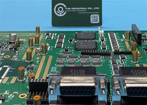
The PCB assembly layer refers to the specific layers within a PCB that are dedicated to the placement and interconnection of electronic components. These layers are typically composed of conductive copper traces, insulating substrates, and solder masks. The assembly layer is where the components are mounted, either through surface-mount technology (SMT) or through-hole technology (THT), and where the electrical connections are made.
2. Types of PCB Assembly Layers
There are several types of PCB assembly layers, each serving a distinct purpose in the overall design and functionality of the PCB:
2.1. Top and Bottom Layers
The top and bottom layers of a PCB are the primary assembly layers where most of the components are placed. These layers are typically used for surface-mount components, which are soldered directly onto the surface of the PCB. The top layer is often referred to as the “component side,” while the bottom layer is known as the “solder side.”
2.2. Inner Layers
Inner layers are used in multi-layer PCBs to provide additional routing space for electrical connections. These layers are sandwiched between the top and bottom layers and are not accessible for component placement. Inner layers are essential for complex designs that require a high density of interconnections.
2.3. Power and Ground Planes
Power and ground planes are specialized layers within a PCB that are dedicated to distributing power and ground signals throughout the board. These layers are typically solid copper planes that provide low-impedance paths for power and ground connections, reducing noise and improving the overall performance of the circuit.
2.4. Solder Mask Layer
The solder mask layer is a protective coating applied over the copper traces to prevent solder bridges and short circuits during the assembly process. This layer also provides insulation and protects the copper traces from environmental factors such as moisture and oxidation.
2.5. Silkscreen Layer
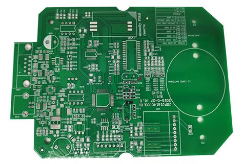
The silkscreen layer is used to print component outlines, reference designators, and other identifying information on the PCB. This layer aids in the assembly process by providing visual guidance for component placement and orientation.
3. Design Considerations for PCB Assembly Layers
Designing the PCB assembly layer requires careful consideration of various factors to ensure the reliability, functionality, and manufacturability of the final product. Some of the key design considerations include:
3.1. Component Placement
Proper component placement is crucial for optimizing the performance and manufacturability of the PCB. Components should be placed in a way that minimizes signal interference, reduces the length of critical signal paths, and facilitates efficient soldering during the assembly process.
3.2. Routing and Trace Width
The routing of electrical connections and the width of the traces are critical factors that impact the electrical performance of the PCB. Proper routing ensures that signals are transmitted with minimal loss and interference, while appropriate trace widths help manage current carrying capacity and thermal dissipation.
3.3. Thermal Management
Thermal management is an essential consideration in PCB design, especially for high-power components. Proper placement of thermal vias, heat sinks, and copper pours can help dissipate heat effectively, preventing overheating and ensuring the longevity of the components.
3.4. Signal Integrity
Signal integrity is a critical aspect of PCB design, particularly for high-speed circuits. Proper layer stacking, controlled impedance routing, and careful placement of decoupling capacitors can help maintain signal integrity and reduce electromagnetic interference (EMI).
3.5. Manufacturability
Designing for manufacturability (DFM) is essential to ensure that the PCB can be assembled efficiently and reliably. This includes considerations such as component spacing, solder mask clearances, and the use of standard component sizes and footprints.
4. The Impact of PCB Assembly Layers on Functionality and Reliability
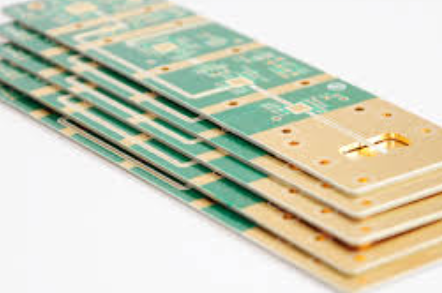
The design and arrangement of the PCB assembly layers have a significant impact on the functionality and reliability of the final product. A well-designed assembly layer ensures that the electrical connections are reliable, the components are properly placed, and the overall performance of the circuit is optimized.
4.1. Electrical Performance
The electrical performance of a PCB is directly influenced by the design of the assembly layers. Proper routing, trace width, and layer stacking can minimize signal loss, reduce crosstalk, and ensure that the circuit operates as intended. Poorly designed assembly layers can lead to signal degradation, increased EMI, and reduced overall performance.
4.2. Thermal Performance
Effective thermal management is critical for the reliability of a PCB, especially in high-power applications. Properly designed assembly layers can help dissipate heat efficiently, preventing thermal stress on components and reducing the risk of failure due to overheating.
4.3. Mechanical Stability
The mechanical stability of a PCB is influenced by the arrangement of the assembly layers. Proper layer stacking and the use of appropriate materials can enhance the mechanical strength of the board, reducing the risk of warping, cracking, or other mechanical failures.
4.4. Manufacturability and Yield
A well-designed assembly layer can improve the manufacturability of the PCB, leading to higher yields and lower production costs. Proper component placement, solder mask clearances, and adherence to DFM guidelines can reduce the likelihood of assembly defects and improve the overall quality of the final product.
5. Advanced Techniques in PCB Assembly Layer Design
As electronic devices become more complex and miniaturized, advanced techniques in PCB assembly layer design are becoming increasingly important. Some of these techniques include:
5.1. High-Density Interconnect (HDI) PCBs
HDI PCBs are designed to accommodate a higher density of components and interconnections in a smaller area. This is achieved through the use of microvias, finer trace widths, and thinner dielectric materials. HDI PCBs are commonly used in smartphones, tablets, and other compact electronic devices.
5.2. Embedded Components
Embedded component technology involves placing passive components, such as resistors and capacitors, within the layers of the PCB. This technique can reduce the overall size of the PCB, improve electrical performance, and enhance thermal management.
5.3. Flexible and Rigid-Flex PCBs
Flexible and rigid-flex PCBs are designed to bend and flex, making them ideal for applications where space is limited or where the PCB needs to conform to a specific shape. These PCBs are commonly used in wearable devices, medical equipment, and aerospace applications.
5.4. 3D Printing of PCBs
3D printing technology is being explored as a potential method for creating PCBs with complex geometries and custom shapes. This technique could revolutionize PCB manufacturing by enabling rapid prototyping and the production of highly customized designs.
6. Conclusion
The PCB assembly layer is a critical aspect of the PCB design and manufacturing process. It determines the arrangement and connectivity of components on the board, impacting the electrical performance, thermal management, mechanical stability, and manufacturability of the final product. As electronic devices continue to evolve, advanced techniques in PCB assembly layer design, such as HDI PCBs, embedded components, and flexible PCBs, are becoming increasingly important. By understanding the intricacies of the PCB assembly layer and considering the various design factors, engineers can create reliable, high-performance PCBs that meet the demands of modern electronic applications.
In conclusion, the PCB assembly layer is not just a physical layer on the board; it is the foundation upon which the entire electronic device is built. A well-designed assembly layer ensures that the device functions as intended, while a poorly designed one can lead to a host of issues, from signal degradation to mechanical failure. As such, the importance of the PCB assembly layer cannot be overstated, and it is essential for engineers to give it the attention it deserves during the design process.