
PCB Assembly Prototyping: A Comprehensive Guide
Introduction
Printed Circuit Board (PCB) assembly prototyping is a critical phase in the development of electronic devices. It involves the creation of a small batch of PCBs to test and validate the design before moving to full-scale production. This process ensures that the design is functional, reliable, and ready for mass manufacturing. PCB assembly prototyping is a complex process that requires careful planning, precise execution, and thorough testing. This article will delve into the various aspects of PCB assembly prototyping, including its importance, the steps involved, the technologies used, and the challenges faced.
The Importance of PCB Assembly Prototyping
- Design Validation: Prototyping allows engineers to validate the design of the PCB. It helps in identifying any design flaws or errors that could lead to malfunctions or failures in the final product. By testing the prototype, engineers can make necessary adjustments to the design before it goes into mass production.
- Functionality Testing: Prototyping provides an opportunity to test the functionality of the PCB. Engineers can verify that all components are working as intended and that the PCB performs its intended functions correctly. This step is crucial in ensuring that the final product will meet the required specifications and performance standards.
- Cost Efficiency: Identifying and fixing issues during the prototyping phase is much more cost-effective than making changes during mass production. Prototyping helps in minimizing the risk of costly errors and rework, ultimately saving time and money.
- Time-to-Market: Prototyping accelerates the development process by allowing engineers to quickly iterate and refine the design. This helps in reducing the time-to-market, giving companies a competitive edge in the fast-paced electronics industry.
- Risk Mitigation: Prototyping helps in mitigating risks associated with new designs and technologies. By testing the prototype, engineers can identify potential risks and take proactive measures to address them before they become major issues in the final product.
Steps Involved in PCB Assembly Prototyping
- Design and Layout: The first step in PCB assembly prototyping is the design and layout of the PCB. This involves creating a schematic diagram that outlines the electrical connections between components. The schematic is then converted into a physical layout using PCB design software. The layout defines the placement of components, routing of traces, and the overall structure of the PCB.
- Component Selection: Once the design is finalized, the next step is to select the components that will be used in the PCB. This includes choosing the right resistors, capacitors, integrated circuits, connectors, and other electronic components. The selection of components is critical as it directly impacts the performance, reliability, and cost of the PCB.
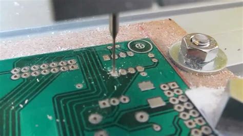
- PCB Fabrication: After the design and component selection, the next step is PCB fabrication. This involves creating the physical PCB based on the design layout. The fabrication process includes several steps such as etching, drilling, plating, and soldering. The result is a bare PCB that is ready for component assembly.
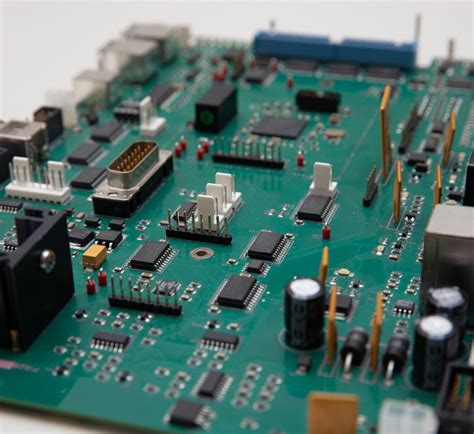
- Component Assembly: The next step is to assemble the components onto the PCB. This can be done using either through-hole technology (THT) or surface-mount technology (SMT). THT involves inserting component leads through holes in the PCB and soldering them on the opposite side. SMT involves placing components directly onto the surface of the PCB and soldering them in place. Both methods have their advantages and are chosen based on the specific requirements of the design.
- Testing and Validation: Once the components are assembled, the PCB undergoes testing and validation. This includes functional testing, where the PCB is powered up and its performance is evaluated. It also includes environmental testing, where the PCB is subjected to various conditions such as temperature, humidity, and vibration to ensure its reliability. Any issues identified during testing are addressed, and the design is refined as necessary.
- Iteration and Refinement: Based on the results of testing and validation, the design may undergo several iterations and refinements. This involves making changes to the design, fabricating new prototypes, and retesting until the desired performance and reliability are achieved.
Technologies Used in PCB Assembly Prototyping
- Computer-Aided Design (CAD) Software: CAD software is used to create the schematic and layout of the PCB. It allows engineers to design the PCB with precision and accuracy, ensuring that all components are properly placed and connected.
- Automated Optical Inspection (AOI): AOI is used to inspect the PCB for defects such as missing components, misaligned components, and soldering defects. It uses cameras and image processing algorithms to detect and identify any issues in the assembly.
- X-Ray Inspection: X-ray inspection is used to inspect the internal structure of the PCB, particularly for complex designs with hidden solder joints. It helps in identifying defects such as voids, cracks, and insufficient solder.
- In-Circuit Testing (ICT): ICT is used to test the electrical performance of the PCB. It involves using a bed of nails fixture to make contact with specific points on the PCB and measure the electrical signals. ICT helps in identifying issues such as short circuits, open circuits, and incorrect component values.
- Functional Testing: Functional testing involves powering up the PCB and evaluating its performance. It includes testing the functionality of individual components, as well as the overall performance of the PCB. Functional testing helps in ensuring that the PCB meets the required specifications and performance standards.
- Environmental Testing: Environmental testing involves subjecting the PCB to various conditions such as temperature, humidity, and vibration. It helps in evaluating the reliability and durability of the PCB under different environmental conditions.
Challenges in PCB Assembly Prototyping
- Design Complexity: As electronic devices become more complex, so do the PCBs that power them. Designing a PCB with a high level of complexity requires advanced skills and expertise. It also increases the risk of design errors and manufacturing defects.
- Component Availability: The availability of components can be a challenge in PCB assembly prototyping. Some components may be difficult to source, especially for custom or specialized designs. This can lead to delays in the prototyping process and impact the overall timeline.
- Cost Management: PCB assembly prototyping can be expensive, especially for small batches. Managing costs while ensuring high-quality prototypes is a challenge that requires careful planning and budgeting.
- Time Constraints: Time is a critical factor in PCB assembly prototyping. Companies are often under pressure to bring products to market quickly, which can lead to rushed prototyping and increased risk of errors.
- Quality Assurance: Ensuring the quality of the prototype is a major challenge. Any defects or issues in the prototype can lead to costly rework and delays. Implementing rigorous quality assurance processes is essential to minimize the risk of defects.
Conclusion
PCB assembly prototyping is a vital step in the development of electronic devices. It allows engineers to validate the design, test functionality, and identify potential issues before moving to mass production. The process involves several steps, including design and layout, component selection, PCB fabrication, component assembly, testing and validation, and iteration and refinement. Various technologies, such as CAD software, AOI, X-ray inspection, ICT, functional testing, and environmental testing, are used to ensure the quality and reliability of the prototype.
Despite the challenges, PCB assembly prototyping offers numerous benefits, including design validation, functionality testing, cost efficiency, time-to-market acceleration, and risk mitigation. By carefully managing the prototyping process and addressing the challenges, companies can ensure the successful development of high-quality electronic products.
In conclusion, PCB assembly prototyping is a complex but essential process that plays a crucial role in the development of electronic devices. It requires a combination of technical expertise, advanced technologies, and careful planning to achieve the desired results. By investing in a robust prototyping process, companies can minimize risks, reduce costs, and bring innovative products to market more efficiently.