
PCB Design for Crystal Oscillator Packaging: Best Practices and Considerations
Introduction
Crystal oscillators serve as the heartbeat of modern electronic systems, providing precise timing references for microcontrollers, processors, and communication interfaces. The packaging and PCB design surrounding these critical components significantly impact system performance, reliability, and electromagnetic compatibility. This 2000-word article explores comprehensive design considerations for implementing crystal oscillator packages on printed circuit boards, covering fundamental principles, layout techniques, and advanced optimization strategies.
Fundamental Concepts of Crystal Oscillator Operation
Quartz Crystal Physics
At the core of most oscillators lies a quartz crystal that vibrates at a specific resonant frequency when properly excited. The piezoelectric properties of quartz cause it to generate an electric potential when mechanical stress is applied, and conversely, to deform when an electric field is present. This bidirectional energy conversion enables sustained oscillation when connected in an appropriate circuit.
Equivalent Circuit Model
Engineers model crystals using an equivalent circuit containing:
- Motional inductance (L₁): Represents the crystal mass
- Motional capacitance (C₁): Represents crystal stiffness
- Shunt capacitance (C₀): Represents electrode capacitance
- Series resistance (R₁): Represents energy losses
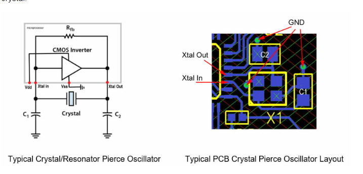
Understanding this model proves essential for proper PCB implementation, as parasitic elements in the layout can significantly alter circuit behavior.
Crystal Oscillator Package Types
Through-Hole Packages
- HC-49/U: The classic “full size” through-hole package measuring approximately 11mm x 4mm
- HC-49/S: “Low profile” version about half the height of HC-49/U
- UM Series: Smaller cylindrical packages for through-hole mounting
Surface Mount Packages
- SMD3225: 3.2mm x 2.5mm footprint (common for 12-54MHz)
- SMD2520: 2.5mm x 2.0mm (higher frequency applications)
- SMD2016: 2.0mm x 1.6mm (space-constrained designs)
- SMD1612: 1.6mm x 1.2mm (ultra-compact applications)
Integrated Oscillator Modules
Fully-contained solutions incorporating the crystal, sustaining circuitry, and sometimes voltage regulation in single packages. These simplify design but offer less flexibility than discrete crystals.
Critical PCB Layout Considerations
Component Placement Strategy
- Proximity to Load Device: Place the crystal within 5-10mm of the target IC’s oscillator pins
- Orientation: Align crystal parallel to PCB edges to minimize board stress effects
- Clearance: Maintain at least 2x package height clearance from board edges
- Layer Consideration: Preferably place on top layer with solid ground plane beneath
Trace Routing Fundamentals
- Length Matching: Keep traces to XTAL_IN and XTAL_OUT as equal as possible
- Width Control: Use 8-15 mil traces for most applications
- Impedance: Not typically critical for low-frequency crystals (<25MHz)
- Corners: Use 45° angles or curves rather than 90° turns
Grounding Techniques
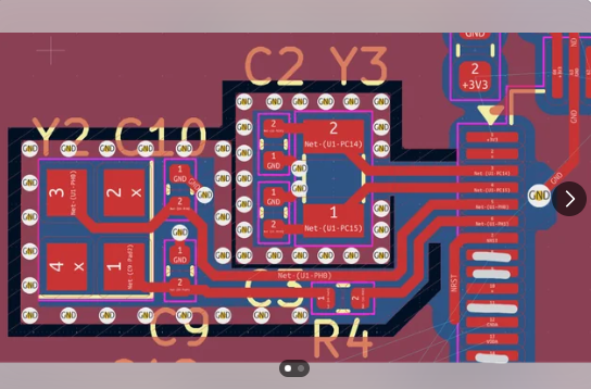
- Local Ground Plane: Implement a dedicated ground area under the oscillator circuit
- Via Placement: Use multiple ground vias near the crystal to reduce loop area
- Isolation: Consider a ground moat around sensitive oscillator circuits
- Return Paths: Ensure uninterrupted ground return paths beneath oscillator traces
Parasitic Management
Stray Capacitance Control
- Trace Separation: Maintain ≥3x trace width spacing between oscillator traces
- Layer Stacking: Avoid routing other signals directly above/below oscillator traces
- Shielding: Use grounded copper pour between oscillator and noisy circuits
Inductive Effects Mitigation
- Loop Area Minimization: Keep current paths as compact as possible
- Via Optimization: Use multiple vias in parallel for lower inductance
- Component Selection: Choose packages with minimal internal inductance
Power Supply Considerations
Decoupling Strategy
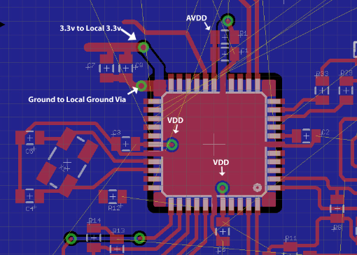
- Local Decoupling: Place 100nF ceramic capacitor within 2mm of oscillator VCC pin
- Bulk Capacitance: Add 1-10µF tantalum or ceramic capacitor nearby
- Ferrite Beads: Consider using for additional power rail filtering
Voltage Regulation
- LDO Selection: Choose low-noise regulators for oscillator power
- Isolation Resistors: Implement series resistors for critical oscillator supplies
- Reference Planes: Maintain clean power planes for oscillator circuits
Load Capacitance Implementation
Calculation Methodology
The total load capacitance (CL) seen by the crystal must match the manufacturer’s specification:
1/CL = 1/C1 + 1/C2 + Cstray
Where C1 and C2 are the external load capacitors and Cstray represents PCB parasitic capacitance (typically 2-5pF).
Practical Implementation
- Capacitor Selection: Use NP0/C0G dielectric capacitors for best stability
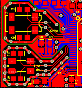
- Placement: Position load capacitors as close as possible to the crystal
- Adjustment: May require experimentation to achieve exact target frequency
EMI Reduction Techniques
Radiation Control
- Guard Rings: Implement grounded copper traces around oscillator
- Shielding Cans: Consider metal shields for critical applications
- Layer Management: Route oscillator traces on inner layers when possible
Harmonic Suppression
- Filtering: Add series resistors (10-100Ω) to oscillator traces
- Termination: Implement appropriate termination for clock distribution
- Buffer Selection: Use slew-rate controlled clock buffers
Thermal Considerations
Temperature Stability
- Material Selection: Choose crystals with appropriate temperature coefficients
- Placement: Avoid proximity to heat-generating components
- Isolation: Consider thermal relief cuts for sensitive oscillators
Board Stress Effects
- Mounting: Avoid placing near board flex points
- Adhesives: Use minimal underfill for SMD crystals
- Mechanical Isolation: Implement stress relief in board layout
Manufacturing and Assembly Factors
Solder Joint Reliability
- Pad Design: Follow IPC-7351 guidelines for package-specific footprints
- Stencil Design: Optimize aperture sizes for proper solder volume
- Inspection: Include test points for post-assembly verification
Rework Considerations
- Thermal Mass: Account for crystal sensitivity to heat during rework
- Cleaning: Avoid ultrasonic cleaning that may damage crystals
- Handling: Implement ESD protection during assembly
Testing and Validation
Frequency Verification
- Probe Selection: Use low-capacitance active probes
- Measurement Technique: Account for probe loading effects
- Environmental Testing: Validate across temperature ranges
Signal Integrity Analysis
- Oscilloscope Setup: Use proper grounding techniques
- Rise/Fall Time: Verify meets system requirements
- Jitter Measurement: Assess timing stability
Advanced Techniques
MEMS Oscillator Implementation
- Package Differences: Understand MEMS-specific requirements
- Startup Time: Optimize for fast-start applications
- Shock/Vibration: Leverage MEMS advantages in harsh environments
Low-Power Design
- Current Optimization: Select appropriate drive level
- Startup Circuitry: Implement proper power sequencing
- Mode Switching: Consider oscillator disable features
Troubleshooting Common Issues
Startup Problems
- Load Capacitance: Verify correct values are installed
- Gain Margin: Check oscillator circuit provides sufficient gain
- ESD Damage: Test for electrostatic discharge effects
Frequency Inaccuracy
- Stray Capacitance: Measure and compensate for PCB parasitics
- Load Resistors: Verify proper DC bias conditions
- Aging Effects: Account for long-term crystal parameter shifts
Future Trends
- Higher Frequencies: Design considerations for >100MHz fundamental mode crystals
- Miniaturization: Challenges with 01005 and smaller packages
- Integrated Solutions: System-in-package oscillator implementations
Conclusion
Proper PCB design for crystal oscillator packaging requires careful attention to electrical, mechanical, and thermal considerations. By implementing the techniques discussed—including optimized component placement, parasitic control, proper grounding, and thorough validation—designers can achieve reliable, high-performance oscillator circuits. As electronic systems continue advancing, these fundamental principles will remain essential while adapting to new package technologies and application requirements.