
PCB Design for Electric Vehicle (EV) Charging Stations
EV charging infrastructure accounts for 15% of global electric vehicle investment, with charging station installations growing at 35% annually. PCB failures in charging systems cause 25% of unplanned downtime, primarily from thermal stress, power transient damage, and communication protocol errors under high-power cycling conditions.
If you want to design reliable PCB systems for EV charging stations, then you will need to understand high-power handling requirements, IEC 61851 safety standards, communication protocols like CCS and CHAdeMO, thermal management strategies, and EMI mitigation techniques for outdoor environments.
This guide covers PCB design considerations for EV charging stations, including power electronics layout, safety isolation requirements, thermal solutions, and manufacturing specifications that ensure reliable operation in demanding automotive infrastructure applications.
High-Power PCB Requirements
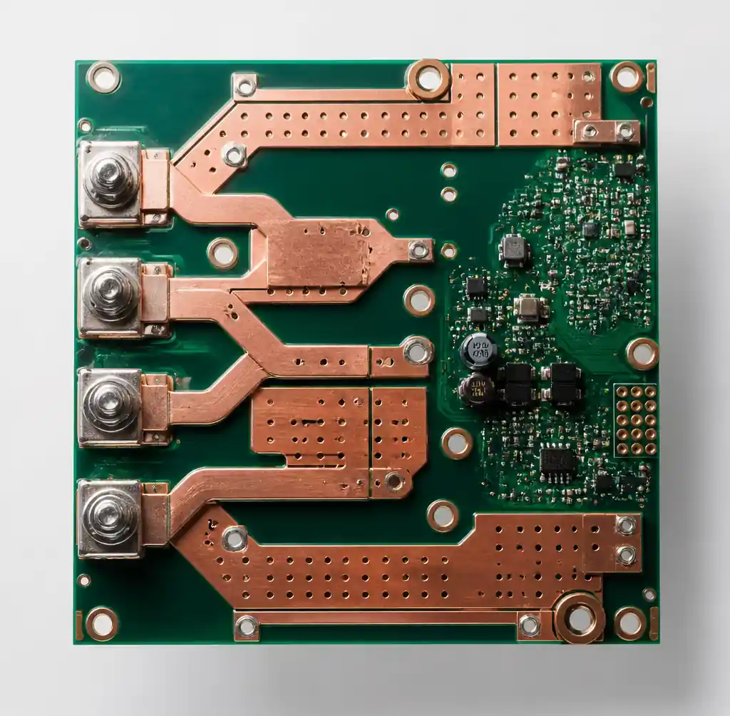
EV charging stations handle power levels from 7kW (Level 2) to 350kW (DC fast charging). PCBs in charging infrastructure manage AC-DC conversion, power factor correction, DC-DC conversion, and battery communication. Power electronics boards operate at currents exceeding 400A for fast chargers, requiring specialized copper weights and thermal design.
For 50kW DC charging systems, power conversion PCBs typically use 4oz to 6oz copper weight to handle 125A continuous current. Bus bar connections replace standard traces for currents above 100A. Current density limits of 30-40A per mm² of cross-section for 4oz copper prevent excessive I²R heating. You should specify metal core PCB for power stages dissipating more than 100W to achieve thermal conductivity of 1-3 W/m·K.
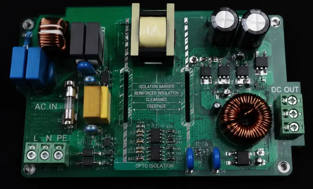
High-voltage isolation separates mains input (up to 480VAC three-phase) from DC output (200-1000VDC). IPC-2221 specifies minimum 0.25mm clearance per 500V working voltage, meaning 600V systems require 0.3mm minimum clearance. Reinforced isolation for safety-critical circuits demands 8mm creepage distance for 400V AC applications.
| Power Level | Current Range | Copper Weight | PCB Type | Thermal Solution |
|---|---|---|---|---|
| 7kW Level 2 | 30A | 2-3oz | Standard multilayer | FR-4 with thermal vias |
| 22kW Level 2 | 90A | 4oz | Heavy copper | Metal core or thick FR-4 |
| 50kW DC Fast | 125A | 4-6oz | Metal core | Aluminum substrate |
| 150kW+ DC | 400A+ | Bus bars | Hybrid rigid-flex | Active cooling required |
IEC 61851 Safety Standards
IEC 61851 defines safety requirements for EV charging systems, covering electrical safety, ground fault protection, and control pilot signaling. PCB designs must meet reinforced insulation requirements between primary AC mains and secondary DC output circuits, with minimum creepage distances of 8mm for 300V AC working voltage per IEC 60664-1 Pollution Degree 2 environments.
Ground fault detection circuits monitor leakage current below 20mA for DC charging systems per IEC 61851-1. Current sense resistors (typically 0.5mΩ to 2mΩ) connect in series with ground return, requiring Kelvin sensing to eliminate measurement errors from high currents. Place sense amplifiers within 50mm of shunt resistors to reduce noise pickup.
Control pilot circuits implement PWM signaling at 1kHz with ±12V amplitude for vehicle state communication. Isolation between control pilot and power circuits uses optocouplers rated 2500V minimum isolation per IEC 61851-1 requirements. Automotive-grade optocouplers like HCPL-3120 provide 5000V isolation with 10MΩ minimum isolation resistance over temperature.
Safety interlocks monitor door position, emergency stop, and ground continuity. Relay control circuits for contactors handling 400A require PCB traces rated for inrush currents of 10× steady state during 100ms closing periods. Automotive relays like TE Connectivity EV200 series require robust driver circuits with flyback protection diodes rated 600V for inductive kick suppression.
Communication Protocol Integration
EV charging stations implement multiple communication protocols: Control Pilot (IEC 61851-1), CCS (Combined Charging System) with PLC over power line, CHAdeMO CAN bus communication, and backend OCPP (Open Charge Point Protocol) over Ethernet or cellular.
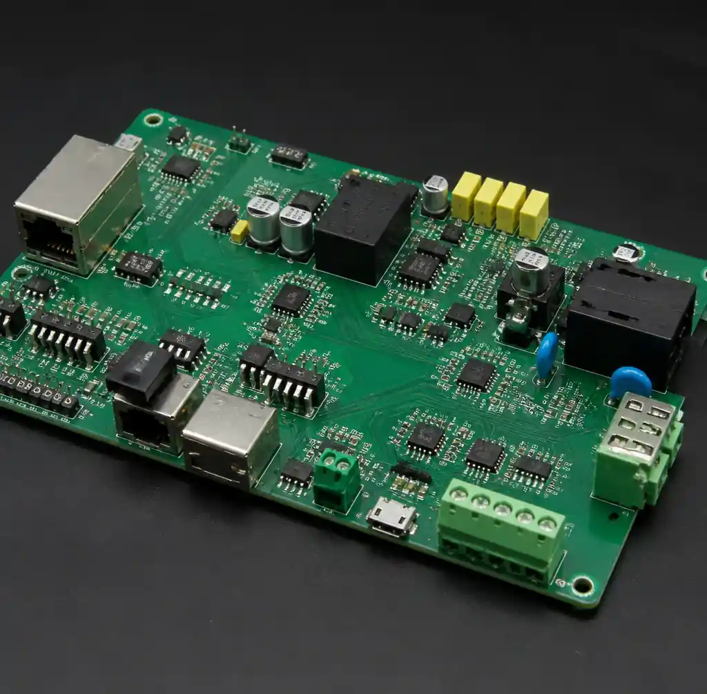
CCS communication uses HomePlug Green PHY powerline communication modulated onto DC charging conductors. Signal coupling circuits must maintain 1MΩ DC isolation while passing 2-30 MHz PLC signals. Coupling capacitors (typically 1µF 2kV rated) block DC voltage while passing communication signals. EMI filtering prevents PLC signals from radiating or interfering with nearby electronics.
CHAdeMO systems use CAN bus at 250kbps or 500kbps for vehicle-to-charger communication. CAN transceiver placement follows standard automotive practices: place transceiver IC within 100mm of connector, use 120Ω termination resistors at each bus end, and maintain differential trace impedance of 120Ω ±10%. Isolated CAN transceivers like ISO1042 provide 2500V isolation between charging controller and vehicle communication.
| Protocol | Physical Layer | Isolation Required | PCB Considerations |
|---|---|---|---|
| Control Pilot (IEC 61851) | PWM ±12V | 2500V minimum | Optocoupler isolation, RC filtering |
| CCS PLC | HomePlug 2-30 MHz | 1MΩ DC isolation | High-voltage coupling caps, EMI filters |
| CHAdeMO CAN | CAN bus 250-500 kbps | 2500V minimum | Isolated CAN, 120Ω termination |
| OCPP Backend | Ethernet or LTE | Optional | Standard networking, surge protection |
Backend communication typically uses Ethernet (10/100Mbps) with OCPP protocol over TCP/IP. Ethernet magnetics provide 1500V isolation per IEEE 802.3. Surge protection (TVS diodes rated 10kV per IEC 61000-4-5) protects communication ports from outdoor lightning-induced transients.
Thermal Management Design
Power conversion efficiency of 95-97% in EV chargers means 1.5kW to 15kW of heat dissipation for 50kW to 350kW systems. Power semiconductors (IGBTs, MOSFETs, diodes) generate concentrated heat loads requiring advanced thermal management beyond standard FR-4 PCB capabilities.
Metal core PCBs using aluminum substrates (1-3 W/m·K thermal conductivity) replace FR-4 (0.3 W/m·K) for power stages. Thermal interface material thickness of 50-100µm separates copper circuit layer from aluminum base. For 150W power module on 100mm × 100mm board area, aluminum substrate limits junction temperature rise to 40°C versus 85°C for standard FR-4 construction.
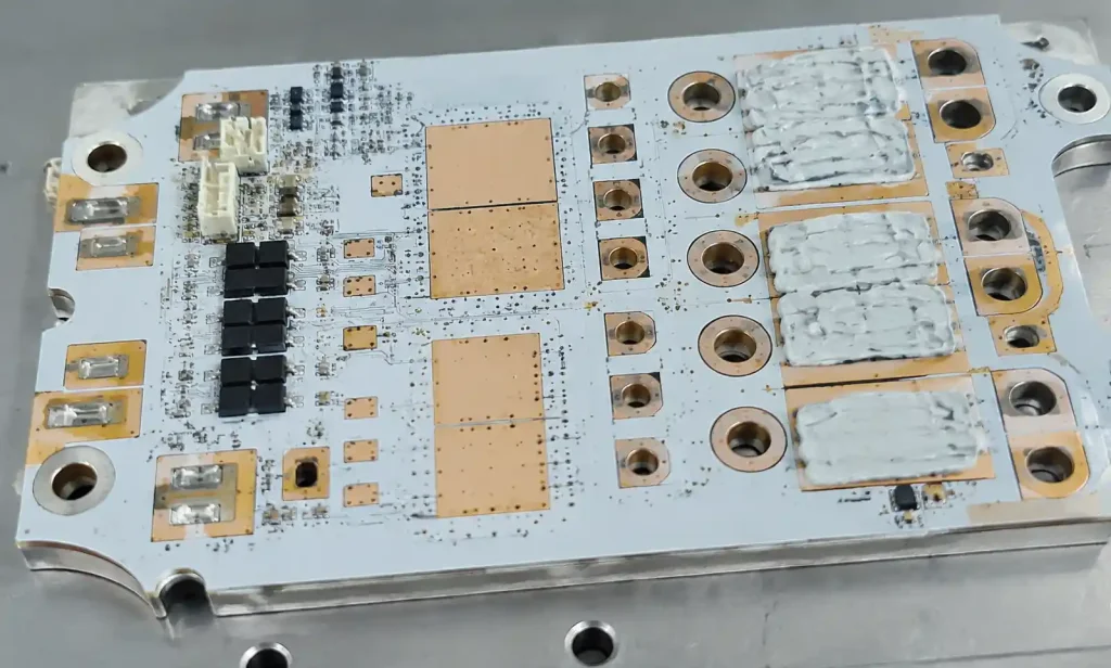
Thermal via arrays under power components transfer heat to ground planes and heat sinks. Via diameter of 0.3mm with 0.6mm pitch provides effective thermal conductivity. For SOT-227 power modules dissipating 200W, use minimum 50 thermal vias under device footprint connecting top copper to bottom thermal plane. Fill vias with conductive epoxy to improve thermal transfer by 30%.
Heat sink attachment requires thermal interface material (TIM) with 1-5 W/m·K conductivity. Mounting hole placement around power semiconductors allows direct thermal path to external heat sink. Gap pad materials accommodate 0.1-0.5mm tolerance in board-to-heatsink distance. Active cooling with fans rated 50-100 CFM maintains junction temperatures below 125°C maximum rating during continuous 50kW operation.
EMI Control Strategies
EV charging stations operate in harsh electromagnetic environments with high-power switching at 20-100 kHz and communication signals from 2-30 MHz. Switching power supplies generate differential-mode and common-mode noise requiring multilayer PCB stackups with proper grounding.
Use minimum 6-layer stackup for power conversion boards: signal/control layer, ground plane, power plane, power switching layer, ground plane, signal/control layer. Continuous ground planes on layers 2 and 5 provide low-impedance return paths and shielding between power and control circuits. Keep power switching traces on inner layers sandwiched between ground planes to contain radiated emissions.
Gate drive circuits for IGBTs and MOSFETs generate high di/dt transients. Place gate drivers within 20mm of power semiconductor gates with controlled impedance traces (typically 50Ω). Gate resistors (5-10Ω) slow switching edges to reduce EMI while maintaining acceptable switching losses. Snubber circuits across power switches dampen voltage ringing from parasitic inductance.
Common-mode chokes on AC input filter conducted EMI on power lines. Place CM chokes before rectification stage with X2 capacitors (0.1-1µF, 300VAC rated) and Y1 capacitors (1-10nF, 250VAC rated) forming pi-filters meeting CISPR 11 Class B emission limits. Differential-mode filtering uses LC filters with damping to prevent resonance.
Shield communication circuits from power switching noise. Route CAN bus and PLC signals on dedicated layers with ground plane separation from power traces. Use ferrite beads (1000Ω @ 100 MHz) in series with sensitive analog inputs. Bypass all IC power pins with 0.1µF ceramic capacitors placed within 5mm of pins to suppress high-frequency noise.
Environmental Protection
Outdoor EV charging stations endure temperature extremes (-40°C to +85°C), humidity (95% RH), UV exposure, salt spray, and vibration. PCB material selection, conformal coating, and connector sealing determine long-term reliability in these conditions.
Specify high-Tg FR-4 material (Tg ≥ 170°C) or polyimide for applications exceeding 130°C operating temperature. High-Tg materials maintain mechanical stability and electrical properties at elevated temperatures from solar heating and internal power dissipation. Glass transition temperature below operating temperature causes dimensional changes and delamination risk.
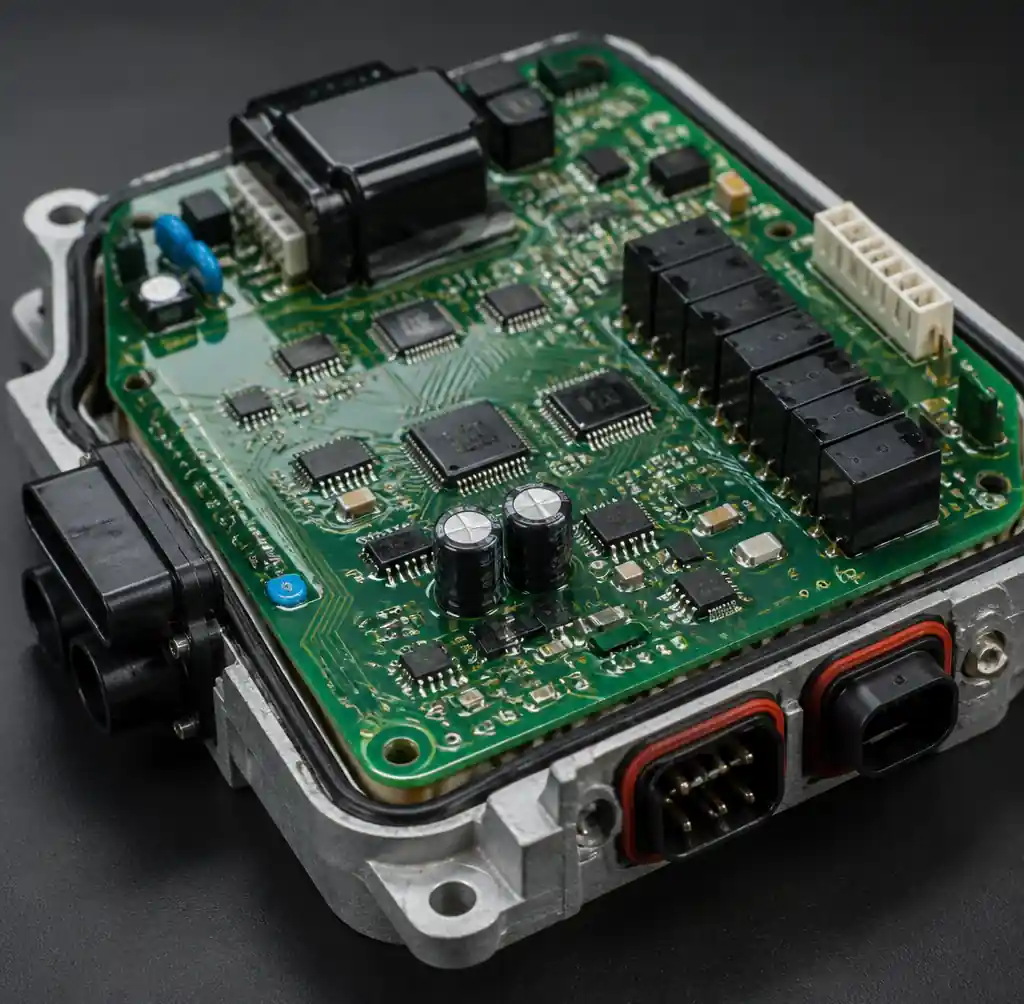
Conformal coating protects PCB assemblies from moisture, dust, and chemical contaminants. Acrylic, silicone, urethane, or parylene coatings provide different protection levels. For automotive applications requiring IP65 or IP67 ingress protection, use urethane or parylene conformal coating with 50-100µm thickness covering all components except high-power devices requiring heat dissipation. Mask areas before coating where thermal interface material contacts board.
Connector selection requires IP67-rated sealed connectors with gaskets for outdoor exposure. High-power DC connectors use copper alloy contacts rated for 1000+ mating cycles at full current. Apply gold plating (0.5-1µm thickness) over nickel base to prevent corrosion in humid environments. Sealed cable entries use strain relief and PG glands to maintain IP rating.
Humidity testing per IPC-TM-650 Method 2.6.3 verifies coating effectiveness. Temperature cycling from -40°C to +85°C for 1000 cycles per AEC-Q200 automotive standard confirms solder joint reliability. Salt spray testing (ASTM B117) for 96-500 hours validates corrosion resistance for coastal installations.
PCB Specifications Comparison
Selecting appropriate PCB technology for EV charging systems depends on power level, thermal requirements, and environmental conditions. The table below compares PCB types commonly specified for different charging station subsystems.
| PCB Type | Layer Count | Max Current | Thermal Performance | Applications | Lead Time |
|---|---|---|---|---|---|
| Standard FR-4 | 4-8 layers | 30A | 0.3 W/m·K | Control boards, Level 2 <10kW | 10-15 days |
| Heavy Copper FR-4 | 6-10 layers | 100A | 0.4 W/m·K | Level 2 22kW, DC 25kW | 15-20 days |
| Metal Core (MCPCB) | 1-4 layers | 200A | 1-3 W/m·K | DC fast charge 50-150kW power stage | 12-18 days |
| Rigid Flex PCB | 4-12 layers | 50A | 0.3-1 W/m·K | Compact designs, cable replacement | 20-25 days |
| Ceramic Substrate | 1-2 layers | 300A | 20-30 W/m·K | Ultra-high power >200kW | 25-30 days |
For control and communication boards handling low power (<100W), standard HDI PCB with 4-6 layers provides sufficient capability. Power distribution and conversion stages require heavy copper or metal core construction. Andwin Circuits manufactures PCBs up to 50 layers with copper weights from 1oz to 6oz, supporting EV charging applications from controller boards to high-power conversion stages.
FAQs
What copper weight is required for 100A DC charging current?
You should specify 4oz (140µm) or 6oz (210µm) copper weight for 100A continuous current. At 4oz copper, use minimum 400-500 mil (10-12mm) trace width to limit temperature rise to 10-15°C above ambient. For higher currents above 150A, consider bus bar connections instead of PCB traces.
How much isolation voltage is required between AC input and DC output?
IEC 61851 requires reinforced insulation with minimum 8mm creepage distance and 3mm clearance for 300V AC working voltage. For 400V AC systems, specify 10mm creepage distance per IEC 60664-1 Pollution Degree 2. Test voltage should be 4000V AC for 1 minute per safety certification requirements.
What PCB material withstands outdoor temperature cycling?
Specify high-Tg FR-4 with glass transition temperature ≥170°C for outdoor applications experiencing -40°C to +85°C cycling. Add conformal coating (urethane or parylene, 50-100µm thickness) for moisture and UV protection. Consider polyimide material for applications exceeding 130°C continuous operating temperature near power semiconductors.
Which PCB type is best for 50kW DC fast charging power stage?
Metal core PCB with aluminum substrate (1-3 W/m·K thermal conductivity) suits 50kW power conversion stages. Use 4oz copper for current handling and thermal vias connecting circuit layer to aluminum base plate for heat transfer to external heat sink. This configuration maintains IGBT junction temperature below 125°C at full power.
How do you design for CCS PLC communication on high-voltage DC lines?
Use high-voltage coupling capacitors (1µF rated 2kV) to pass 2-30 MHz PLC signals while blocking DC voltage. Maintain 1MΩ minimum DC isolation between PLC transceiver and DC power lines. Add EMI filtering to prevent PLC signals from radiating or interfering with control circuits. Follow HomePlug Green PHY specifications for signal coupling.
What thermal management is needed for 350kW ultra-fast charging?
Ultra-fast chargers require active liquid cooling for power semiconductors dissipating 10-15kW of heat. Use metal core PCB with direct copper bonding (DCB) technology on ceramic substrates (20-30 W/m·K). Implement cold plates with water-glycol coolant circulating at 5-10 liters per minute. Junction-to-coolant thermal resistance must stay below 0.1°C/W.
Conclusion
PCB design for EV charging stations requires careful attention to high-power handling, safety isolation per IEC 61851, communication protocol integration, thermal management, and environmental protection. Proper copper weight selection, metal core substrates for power stages, reinforced insulation, and EMI control ensure reliable operation in demanding automotive infrastructure applications.
If you need high-quality PCBs for EV charging systems, Andwin Circuits offers advanced manufacturing capabilities up to 50 layers with heavy copper up to 6oz and fast delivery in 7 days. Our facility is certified to ISO 9001, IATF 16949, and UL standards, ensuring superior quality for power and energy applications. We have successfully delivered PCBs for automotive charging infrastructure, power electronics, and industrial systems worldwide.
Contact us today for custom PCB solutions, technical specifications, and competitive factory-direct pricing for your EV charging station project.