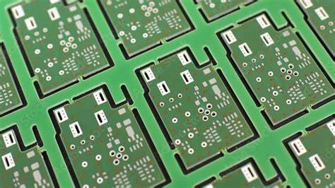
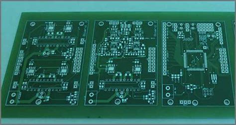
PCB design (layout, layout, routing) specifications for switching power supplies
In modern electronic devices, switching power supplies are widely used due to their high efficiency and compactness. The performance of switching power supplies depends not only on circuit design, but also on the rationality of PCB (Printed Circuit Board) design. Reasonable PCB design specifications, including layout, layout and routing, can effectively improve the stability, efficiency and reliability of switching power supplies, reduce electromagnetic interference (EMI), and reduce production costs.
Layout specifications
Layout of power devices and magnetic components
Power devices (such as switching tubes, diodes, etc.) and magnetic components (such as transformers, inductors, etc.) are the parts of switching power supplies that generate large amounts of heat and have drastic current changes. First of all, power devices and magnetic components should be placed as close as possible to shorten the connection line between them, reduce line resistance and inductance, and thus reduce power loss and electromagnetic interference. For example, in a flyback switching power supply, the distance between the switching tube and the transformer is too far, which will increase the parasitic inductance of the connecting wire, and generate a large voltage spike at the moment when the switching tube is turned off, which will not only affect the life of the switching tube, but also generate strong electromagnetic interference.
Secondly, consider the heat dissipation problem.
Power devices and magnetic components should be placed in the heat dissipation area of the PCB or close to the heat sink. A large area of heat dissipation copper foil can be set under these components to conduct heat to other layers of the PCB through vias to improve the heat dissipation efficiency. At the same time, avoid placing heat-sensitive components (such as some small signal processing chips) near power devices and magnetic components to prevent them from overheating and performance degradation.
Layout of input and output capacitors
Input and output capacitors are crucial for stabilizing the input and output voltages of switching power supplies. The input capacitor should be as close to the power input pin as possible to reduce voltage fluctuations and electromagnetic interference on the input power line. Generally speaking, multiple capacitors with different capacitance values are connected in parallel, such as a large-capacity electrolytic capacitor to filter low-frequency ripple, and a small-capacity ceramic capacitor in parallel to filter high-frequency noise. The pins of these capacitors should be as short as possible to reduce parasitic inductance.
The output capacitor should also be close to the load to ensure the stability of the output voltage. For some applications with high requirements for output voltage accuracy, a small filter inductor can also be added near the load to form an LC filter circuit to further reduce the output ripple.
Layout of control chip
The control chip is the core of the switching power supply, responsible for controlling the on and off of the switch tube. The control chip should be placed in an area away from high-power devices and magnetic components to avoid electromagnetic interference. At the same time, it is necessary to ensure that the power pin of the control chip has a good decoupling capacitor. Usually, a 0.1μF ceramic capacitor and a 10μF electrolytic capacitor are placed near the chip power pin to filter out high-frequency and low-frequency noise on the power line to ensure the stable operation of the control chip.
Layout specification
Functional module division
When PCB layout, the switching power supply should be divided into different functional modules, such as input filter module, power conversion module, output filter module and control module. There should be clear boundaries between each functional module to avoid mutual interference between signals of different modules. For example, the input filter module and the power conversion module can be isolated by a ground plane or routing to prevent the high-frequency noise generated by the power conversion module from entering the input power supply.
Layer planning
For multi-layer PCBs, reasonable layer planning can improve signal integrity and power supply stability. Generally speaking, a dedicated power layer (such as VCC layer) and ground layer (GND layer) are set up. The power layer and ground layer should be placed adjacent to each other, so that a capacitor can be formed, which helps to reduce the noise on the power line. The power signal and the control signal should be transmitted in different layers to avoid mutual interference. For example, the power signal can be transmitted on the top or bottom layer, while the control signal can be transmitted on the middle layer.
Arrangement direction of components
In the same functional module, the arrangement direction of components should be as consistent as possible, which can facilitate wiring and improve the efficiency and quality of wiring. For example, all SMD components such as resistors and capacitors can be arranged in the same direction for easy welding and debugging. At the same time, attention should be paid to the spacing between components, both to ensure that there is enough electrical safety distance between components and to avoid excessive spacing that leads to waste of PCB area.
Routing specifications
Power routing
The power routing needs to withstand large currents, so it needs to have sufficient width. Generally speaking, the width of the power routing is determined by calculation or reference to empirical formulas based on the current size and the thickness of the PCB. For example, for a current of 1A, on an ordinary 1.6mm thick PCB, the trace width is about 1mm. Power traces should be as short and straight as possible, avoiding sharp angles and right angles to reduce the resistance and inductance of the line. When turning is necessary, a 45° angle or rounded corner should be used.
Signal traces
Signal traces must ensure signal integrity and avoid signal distortion and interference. The width of signal traces is generally narrower than that of power traces, and is determined according to the frequency and transmission distance of the signal. For high-frequency signals, microstrip or stripline wiring should be used to control the transmission characteristics of the signal. At the same time, signal traces should be kept away from power traces and magnetic components to avoid electromagnetic interference. Interference can be shielded by setting ground wires on both sides of the signal traces.
Use of vias
Via is an important way to connect different layers of PCB, but vias also introduce parasitic inductance and capacitance. In power traces, in order to ensure smooth transmission of current, multiple vias can be used in parallel to reduce the resistance and inductance of the vias. For high-frequency signals, the size and number of vias should be controlled as much as possible to avoid adverse effects on signal transmission. At the same time, attention should be paid to the connection between the vias and the component pins to ensure reliable connection.
The PCB design specification of the switching power supply is a systematic project. The layout, typesetting and routing need to comprehensively consider electromagnetic compatibility, heat dissipation, signal integrity and other factors. Only by strictly following these specifications can we design a switching power supply PCB with excellent performance, stability and reliability, and provide strong guarantees for the normal operation of electronic equipment. With the continuous development of electronic technology, the requirements for switching power supply PCB design will become higher and higher. Engineers need to constantly learn and explore new design methods and techniques to meet the growing application needs. In the actual design process, professional PCB design software can also be used for simulation and analysis to discover and solve potential problems in advance and improve design efficiency and quality.