
Skip to content
Andwin Circuits
  • Home
  • ProductsExpand
    • HDI multilayer PCB
    • Rigid Flex PCB
    • Flex pcb
    • Special PCBExpand
      • High Frequency PCBExpand
        • Rogers RO4350B PCB
        • Rogers RO4003 pcb
        • Rogers RO3003 PCB
        • Rogers 5880 PCB
        • DICLAD 527 PCB
        • Taconic TLX series
        • Taconic TLX-8 RF PCB
        • Taconic TLX-9 RF PCB
      • High speed pcbExpand
        • Megtron 6 High Speed PCB
        • TU-872 SLK Sp High Speed
      • High TG PCBExpand
        • SHENGYI SH260 PCB
        • ISOLA 370HR PCB
        • ISOLA IS410 PCB
        • ISOLA IS420 PCB
      • Heavy copper PCB
      • Copper coin pcb
      • Copper inlay PCB
    • Metal Core PCBExpand
      • Copper core pcb
      • Aluminum PCB
      • 2 Layers Aluminum PCB
      • Direct thermal MCPCB
      • 2 Layers Direct Thermal
    • Ceramic PCBExpand
      • DPC ceramic PCB
      • DBC ceramic PCB
      • Thick film Ceramic PCB
      • Al2O3 Alumina PCB
      • AIN ALN ceramic PCB
      • IGBT Ceramic PCB
  • ServiceExpand
    • PCB Assembly
    • Quick turn PCB assembly
    • PCBA conformal coating
  • IndustryExpand
    • Telecommunication
    • IoT and Wireless
    • Industrial Control
    • Thermal management
    • Power and Energy
    • IC test board
    • Automative
    • Medical
  • CapabilityExpand
    • Rigid PCB
    • Rigid flex PCB
    • Metal core PCB
    • PCB Assembly
  • TechnologyExpand
    • Blogs
    • Via in pad
    • PCB E-test
    • PCB stack up
    • MCPCB panelization
    • Controlled impedance PCB
  • AboutExpand
    • About us
    • Certification
    • Factory Tour
  • Contact
Andwin Circuits
Home / PCB design whole board copper plating instructions

PCB design whole board copper plating instructions

ByGrace July 12, 2025July 12, 2025

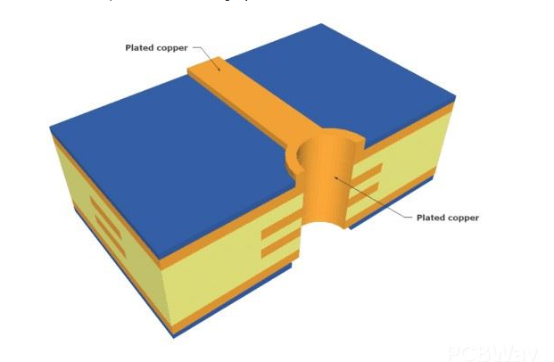
In PCB (printed circuit board) design, whole board copper plating is an issue that needs to be carefully considered. Copper plating, that is, covering the blank area of PCB with copper film, has both significant advantages and potential problems. Whether to plating copper on the whole board needs to be determined according to specific design requirements and circuit characteristics.

1.Advantages of copper plating

    Reduce ground impedance: A large area of copper film can be used as a ground line, significantly reducing ground impedance, which is very important for improving the stability and anti-interference ability of the circuit.

    Reduce electromagnetic interference (EMI): Copper plating can form a continuous shielding layer, effectively reduce electromagnetic interference, and protect sensitive circuits from external electromagnetic fields.

    Enhance heat dissipation performance: Copper has good thermal conductivity, and a large area of copper film can help dissipate the heat generated by components when they are working, improving the stability and life of the equipment.

    Reduce deformation: Copper plating can increase the rigidity of the PCB, reduce deformation caused by temperature changes or mechanical stress, and improve the reliability of the PCB.
    2.Disadvantages of copper plating

      Difficulty in welding and rework: Large areas of copper film may increase the difficulty of welding and rework, especially when local modifications or repairs are required.

      High-frequency signal interference: In high-frequency circuits, copper plating may act as an antenna to introduce additional interference signals, affecting the performance of the circuit.

      Increased cost: Copper plating consumes more copper materials, which may increase the manufacturing cost of PCBs.

      3.Design suggestions for PCBs with different layers

        Two-layer board:

        For two-layer boards, it is usually recommended to lay the ground plane on the bottom layer as the main ground layer.

        The top layer is used to place the main components and run the power and signal lines. Such a design can fully utilize the advantages of copper plating while avoiding interference with the top-layer components and routing.

        Multilayer board:

        In high-speed digital circuits of multilayer boards with complete power and ground planes, copper plating on the outer layer does not bring much benefit.

        On the contrary, the impedance of the microstrip transmission line may be changed due to the coupling between the copper film and the signal line, affecting the signal integrity. Therefore, in the design of multilayer boards, the necessity of copper plating on the outer layer needs to be carefully considered.
        Contact us for PCB quote now |

        4.Treatment of special circuits and areas

          High impedance loops and analog circuits:

          For high impedance loops and analog circuits, copper plating can effectively reduce ground impedance and improve the anti-interference ability and stability of the circuit.

          Therefore, copper plating in these areas is usually beneficial.

          Areas around the antenna part:

          In the area around the antenna part, copper plating is generally not recommended. Because the copper film may introduce additional interference signals as an antenna, or change the radiation characteristics of the antenna, thereby affecting the performance of wireless communication.

          From the above content, it can be seen that in PCB design, whether to plating copper on the entire board needs to consider multiple factors. Including the type of circuit, signal integrity requirements, heat dissipation requirements, and manufacturing costs. For two-layer boards, it is usually recommended to lay the ground plane on the bottom layer; for multi-layer high-speed digital circuits, copper plating on the outer layer needs to be carefully considered; for high impedance loops and analog circuits, copper plating is usually beneficial; and in the area around the antenna part, copper plating is not recommended. Through reasonable design and optimization, the advantages of copper plating can be fully utilized while avoiding its potential problems.

          Contact us for PCB quote now |

          Post Tags: #aluminum clad pcb#aluminum core pcb#aluminum core pcb led#aluminum pcb#assemble pcb

          Post navigation

          Previous Previous
          Analysis of PCB Trace Breakage Causes
          NextContinue
          PCB circuit board corrosion process

          Search

          Search

          Products

          • HDI Multilayer PCB
          • Rigid Flex PCB
          • Flex pcb
          • High Frequency PCB
          • High speed pcb
          • Heavy copper PCB
          • Metal Core PCB
          • Ceramic PCB

          Address

          Andwin Circuits Co.,Limited
          Email: sales@andwinpcb.com
          Tel: +86 755 2832 9394
          Fax:+86 755 2992  6717
          ADD:1-2F-1217,HouDeQun Industrial park,
          NanTing RD NO.56,ShaJing,BaoAn,Shenzhen 518104,GuangDong,China

          Products

          • HDI Multilayer PCB
          • Rigid Flex PCB
          • Flex pcb
          • High Frequency PCB
          • High speed pcb
          • Heavy copper PCB
          • Metal Core PCB
          • Ceramic PCB

          Technology

          • Blogs
          • Via in pad
          • PCB E-test
          • PCB stack up
          • Metal core PCB panelization
          • Controlled impedance PCB

          CERTIFICATION

          Certification >>


          Copyright© 2003 - 2026 Andwin | All Rights Reserved | Powered by Andwin

          Scroll to top
          • Home
          • Products
            • HDI multilayer PCB
            • Rigid Flex PCB
            • Flex pcb
            • Special PCB
              • High Frequency PCB
                • Rogers RO4350B PCB
                • Rogers RO4003 pcb
                • Rogers RO3003 PCB
                • Rogers 5880 PCB
                • DICLAD 527 PCB
                • Taconic TLX series
                • Taconic TLX-8 RF PCB
                • Taconic TLX-9 RF PCB
              • High speed pcb
                • Megtron 6 High Speed PCB
                • TU-872 SLK Sp High Speed
              • High TG PCB
                • SHENGYI SH260 PCB
                • ISOLA 370HR PCB
                • ISOLA IS410 PCB
                • ISOLA IS420 PCB
              • Heavy copper PCB
              • Copper coin pcb
              • Copper inlay PCB
            • Metal Core PCB
              • Copper core pcb
              • Aluminum PCB
              • 2 Layers Aluminum PCB
              • Direct thermal MCPCB
              • 2 Layers Direct Thermal
            • Ceramic PCB
              • DPC ceramic PCB
              • DBC ceramic PCB
              • Thick film Ceramic PCB
              • Al2O3 Alumina PCB
              • AIN ALN ceramic PCB
              • IGBT Ceramic PCB
          • Service
            • PCB Assembly
            • Quick turn PCB assembly
            • PCBA conformal coating
          • Industry
            • Telecommunication
            • IoT and Wireless
            • Industrial Control
            • Thermal management
            • Power and Energy
            • IC test board
            • Automative
            • Medical
          • Capability
            • Rigid PCB
            • Rigid flex PCB
            • Metal core PCB
            • PCB Assembly
          • Technology
            • Blogs
            • Via in pad
            • PCB E-test
            • PCB stack up
            • MCPCB panelization
            • Controlled impedance PCB
          • About
            • About us
            • Certification
            • Factory Tour
          • Contact
          Search